PIONEER CX-938 Service Manual

Cover page of PIONEER CX-938 Service Manual

Service Manual for PIONEER CX-938, downloadable as a PDF file.

Manual details

  • Immediate download after payment.
  • Delivered as a PDF file.
  • The manual has 29 pages
  • File size: 0.61 MB
  • Available language versions: English
  • Different language versions may vary sligthly in file size and page count.

We guarantee that...

  • our manuals are complete,
  • the manual includes circuit diagrams,
  • our manuals are checked with antivirus,
  • We'll issue refund if the manual is damaged, incomplete or unreadable (our refund policy)

Sample pages

Thumbnail of page 1Thumbnail of page 2Thumbnail of page 3Thumbnail of page 4
Thumbnail of page 5Thumbnail of page 6Thumbnail of page 7Thumbnail of page 8
Thumbnail of page 9
background image
Model
Service Manual
CD Mechanism Module
Mechanism Unit
CDX-P1250/X1N/UC,ES
CRT2318
CXK4900
CXB3008
CDX-P1250/X1N/EW
CXK4905
CXB3008
CDX-FM1259/X1N/UC
CRT2320
CXK4916
CXB3008
CDX-FM1257/X1N/UC,ES
CXK4915
CXB3008
PIONEER ELECTRONIC CORPORATION
4-1, Meguro 1-Chome, Meguro-ku, Tokyo 153-8654, Japan
PIONEER ELECTRONICS SERVICE INC.
P.O.Box 1760, Long Beach, CA 90801-1760 U.S.A.
PIONEER ELECTRONIC [EUROPE] N.V.
Haven 1087 Keetberglaan 1, 9120 Melsele, Belgium
PIONEER ELECTRONICS ASIACENTRE PTE.LTD. 253 Alexandra Road, #04-01, Singapore 159936
C PIONEER ELECTRONIC CORPORATION 1999
K-ZZU. FEB. 1999 Printed in Japan
ORDER NO.
CRT2357
CD MECHANISM MODULE
CX-938
- This service manual describes the operation of the CD mechanism incorporated in models listed in the
table below.
- When performing repairs use this manual together with the specific manual for model under repair.
CONTENTS
1. CIRCUIT DESCRIPTIONS ...........................................2
2. DISASSEMBLY .........................................................18
3. MECHANISM DESCRIPTIONS.................................23
background image
2
CX-938
1. CIRCUIT DESCRIPTIONS
The LSI (UPD63710GC) used on this unit comprises five main blocks ; the pre-amp section, servo, signal processor,
DAC and CD text decoder (not used on this model). It also equips with nine automatic adjustment functions.
1.1 PRE-AMP SECTION
This section processes the pickup output signals to
create the signals for the servo, demodulator and
control.
The pickup output signals are I-V converted by the pre-
amp with the built-in photo-detector in the pickup, then
added by the RF amp to obtain RF, FE, TE, TE zero cross
and other signals.
This pre-amp section is built in the servo LSI
UPD63710GC (IC201). The following describes function
of each section.
Since this system has a single power supply (
+5V), the
reference voltage for this LSI and pickup are set to
REFO (2.5V). The REFO is obtained by passing the
REFOUT from the LSI through the buffer amplifier. The
REFO is output from Pin 89 of this LSI. All
measurements are done using this REFO as reference.
Note : During the measurement, do not try to short the
REFO and GND.
1) APC Circuit (Automatic Power Control)
When the laser diode is driven with constant current,
the optical output has large negative temperature
characteristics. Thus, the current must be controlled
from the monitor diode so that the output may be
constant. APC circuit is for it. The LD current is obtained
by measuring the voltage between LD1 and V
+5. The
value of this current is about 35mA.
71
72
74
76
AGCI
77
RFO
75
78
79
80
73
91
90
93
92
C-3T
FEO
FE-
TEO
TE-
85
86
87
E
97
PD
99
PN
F
D
82
83
84
B
C
A
RF-
EQ1
EQ2
AGCO
RFI
ASY
EFM
PEAK DET.
LPF
BOTTOM DET.
S/H
D/A
A/D
D/A
A/D
94
98
TE2
LD
VREG
GND
APN
LDON
EFM
DEFECT
FOK
A3T
MIRR
To the
following stage
of the LSI
Vref
Vref
Vref
Vref
Vref
Vref
Vref
Vref
Vref
Vref
Vref
Vref
Vref
Vref
Vref
·····Vref(+2.5V)
97
PD
99
PN
98
LD
VREG
GND
AMP_PN
(H:Nch L:Pch)
LDON
(H:LD MOVE L:STOP)
Vref
·····Vref(+2.5V)
14
5
R102
10
R101
12
Q101
2SB1132
C102
0.1
µF
C103
100
µF/6.3V
PU UNIT
R103
2.2k
C105
0.33
µF
+5V
1k
110k
3pF
3pF
150k
100k
100k
16k
1k
Fig.1 : BLOCK DIAGRAM OF BUILT-IN RF AMPLIFIER
Fig.2 : APC CIRCUIT
background image
CX-938
3
2) RF Amplifier and RFAGC Amplifier
The photo-detector outputs (A
+ C) and (B + D) are
added, amplified and equalized on this LSI and then
output to the RFI terminal as the RF signal. (The eye
pattern can be checked by this signal.)
The RFI voltage low frequency component is :
RFI = (A
+ B + C + D) × 3.2
RFI is used on the FOK generator circuit and RF offset
adjusting circuit.
R215 is an offset resistor for maintaining the bottom
reference voltage of the RFI signal at 1.5 VDC. The D/A
output used for the RF offset adjustment (to be
described later) is entered via this resistor.
After the RFI signal from Pin 77 is externally AC
coupled, entered to Pin 76 again, then amplified on the
RFAGC amplifier to obtain the RFO signal.
The RFAGC adjustment function (to be described later)
built-in the LSI is used for switching feedback gain of
the RFAGC amplifier so that the RFO output may go to
1.5
± 0.3Vpp.
The RFO signal is used for the EFM, DFCT, MIRR and
RFAGC adjustment circuits.
3) FOK Circuit
This circuit generates the signal that is used for
indicating the timing of closing the focus or state of the
focus close currently being played. This signal is output
from Pin 4 as the FOK signal. It goes high when the
focus close and in-play.
The RFOK signal is generated by holding DC level of the
RFI at its peak with the succeeding digital section, then
comparing it at a specific threshold level. Thus, the
RFOK signal goes high even if the pit is absent. It
indicates that the focus close can take place on the disc
mirror surface, too.
This signal is also supplied to the micro computer via
the low pass filter as the FOK signal and used for the
protection and the RF amplifier gain switching.
CN101
84
18
25
83
82
10k
10k
85
FOK
CIRCUIT
A/D
4
A+C
16k
B+D
10k
16k
10k
R215
12k
C209 3pF
R214
10k
R207
1.8k
C208
27pF
R213
10k
80
79
74
75
76
77
D/A
12k
66
10k
RFO
AGCI
RFI
C207
0.22
µF
C206
3900pF
FOK
TO EFM
CIRCUIT
Fig.3 : RFAMP, RFAGC AND FOK CIRCUIT
background image
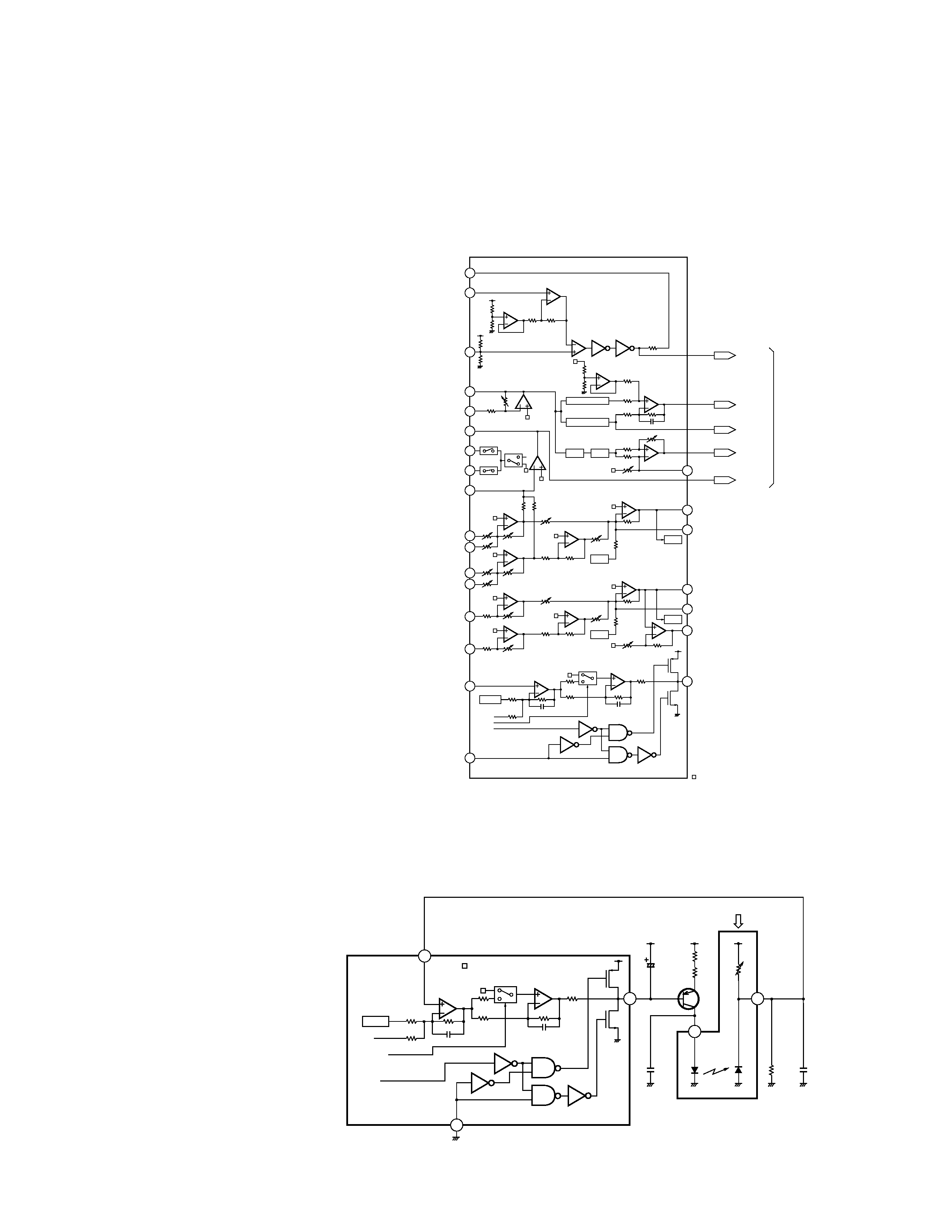
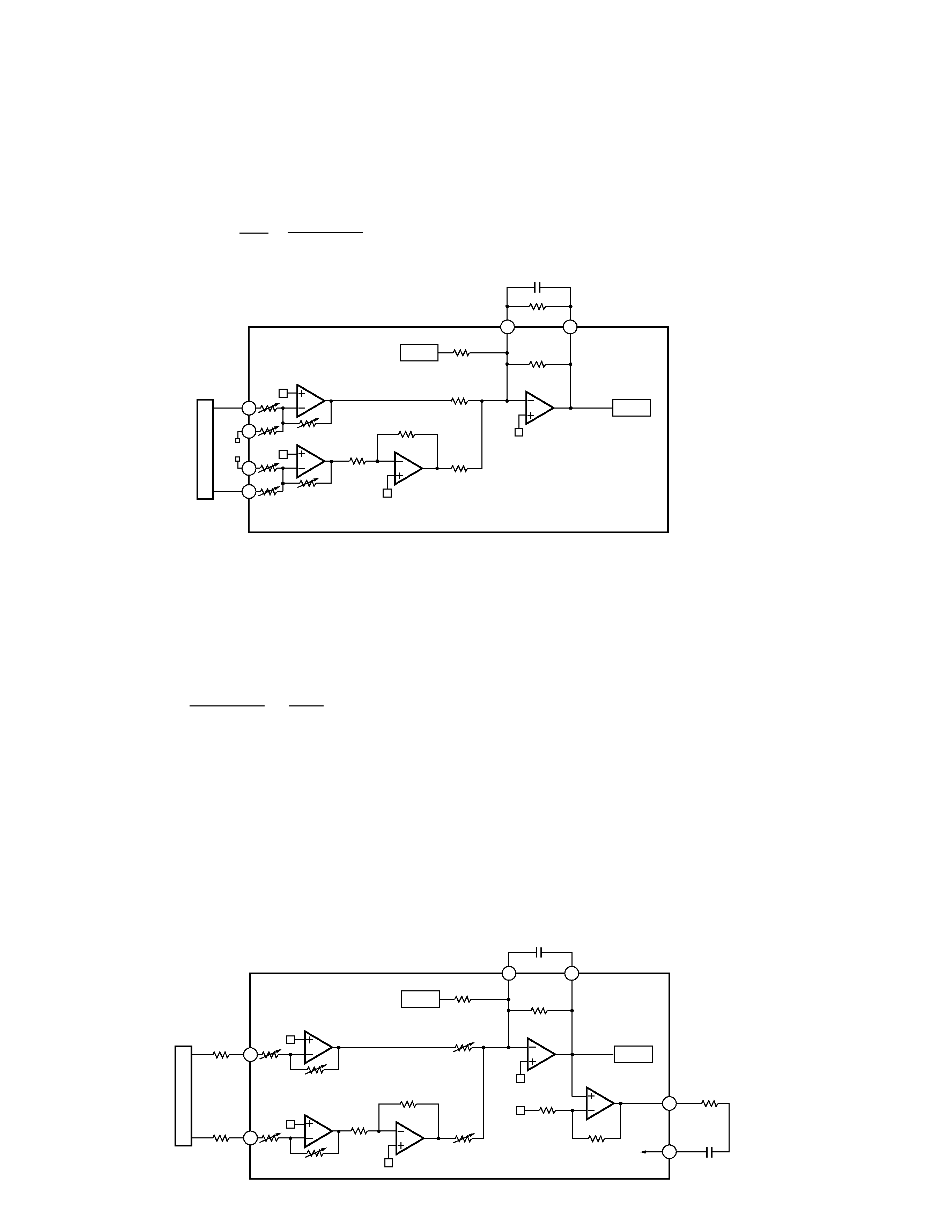
5) Tracking Error Amplifier
The photo-detector outputs E and F are passed through
a differential amplifier and an error amplifier, and then
(E
- F) is output from Pin 93 as the TE signal. The TE
voltage low frequency component is :
TE
= (E - F) ××
= (E - F) × 5.7 (Effective LSI output is 5.0).
Using REFO as the reference, the TE waveform of
approximately 1.3 Vpp is obtained for the TE output.
The final-stage amplifier cutoff frequency is 20 kHz.
6) Tracking Zero Crossing Amplifier
TEC signal (the tracking zero crossing signal) is
obtained by multiplying the TE signal four times. It is
used for locating the zero crossing points of the
tracking error. The zero cross point detection is done for
the following two reasons :
1 To count tracks for carriage moves and track jumps.
2 To detect the direction in which the lens is moving
when the tracking is closed (it is used on the
tracking brake circuit to be described later).
The TEC signal frequency range is 300 Hz to 20 kHz.
TEC voltage
= TE level × 4
Theoretical TEC level is 5.2V. The signal exceeds D-
range of the operational amplifier and thus is clipped.
It, however, can be ignored since this signal is used by
the servo LSI only at the zero crossing point.
4
CX-938
Fig.5 TRACKING ERROR AMPLIFIER AND TRACKING ZERO CROSSING AMPLIFIER
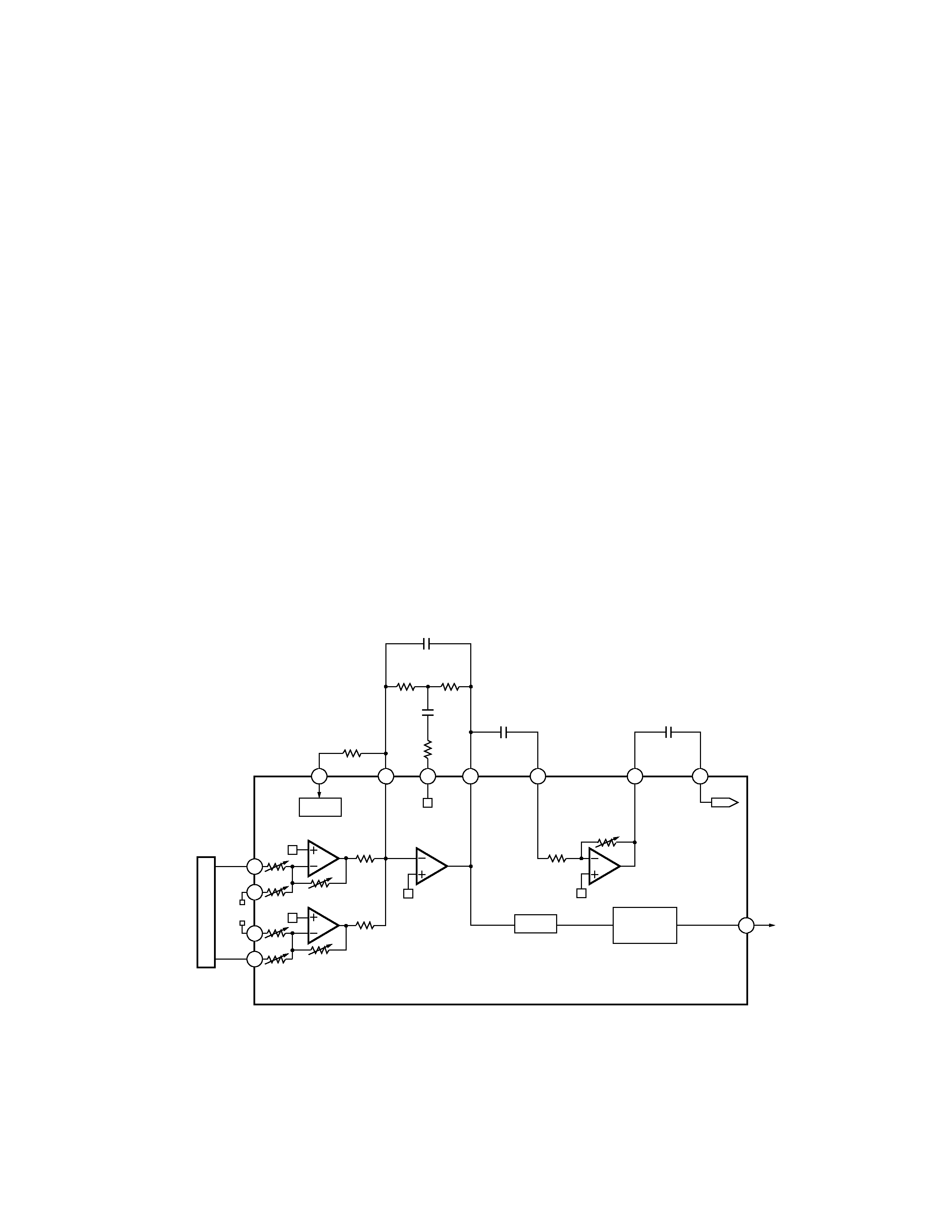
4) Focus Error Amplifier
The photo-detector outputs (A
+ C) and (B + D) are passed
through a differential amplifier and an error amplifier, and
then (A
+ C - B - D) is output from Pin 91 as the FE signal.
The FE voltage low frequency component is :
FE
= (A + C - B - D) ××
= (A + C - B - D) × 5
Using REFO as the reference, an S-curve of approximately 1.5
Vpp is obtained for the FE output. The final-stage amplifier
cutoff frequency is 11.4 kHz.
20k
CN101
84
18
25
83
82
10k
20k
85
A+C
16k
B+D
48k
16k
10k
91
90
D/A
80k
110k
FE
C210 220pF
R208 300k
A/D
FE OFFSET
TO DIG. EQ
48k
38k
CN101
21
23
86
56k
38k
87
F
E
F
224k
E
48k
224k
56k
93
92
D/A
80k
110k
TE
C211 100pF
A/D
TE OFFSET
TO DIG. EQ
48k
R216
27k
R215
27k
60k
20k
95
94
TE2
TEC
R212
0
C212
6800pF
16k
10k
(80k//300k)
20k
Fig.4 : FOCUS ERROR AMPLIFIER
224k
(56k
+27k)
80k
38k
background image
CX-938
7) DFCT (Defect) Circuit
The DFCT signal is used for detecting defects on the
mirrored disc surface. It allows monitoring from the
HOLD pin (Pin 2). It goes high when defects are found
on the mirrored surface.
The DFCT signal is generated by comparing the RF
amplified signal (which is obtained by bottom holding
the RFO signal) at a specific threshold level by the
succeeding digital section.
Stains or scratches on the disc can constitute the
defects on the mirrored disc surface. Thus, as long as
the DFCT signal remains high in the LSI, the focus and
tracking servo drives are held in the current state so
that a better defect prevention may be ensured.
8) 3TOUT Circuit
The 3TOUT signal is generated by entering disturbance
to the focus servo loop, comparing phase of
fluctuations of the RF signal 3T component against that
of the FE signal at that time, then converting the signal
to DC level. This signal is used for adjusting bias of the
FE signal (to be described later). This signal is not
output from the LSI, thus its monitoring is not available.
9) MIRR (Mirror) Circuit
The MIRR signal shows the on track and off track data,
and is output from Pin 3.
When the laser beam is
On track : MIRR
= "L"
Off track : MIRR
= "H"
This signal is used on the brake circuit (to be described
later) and also as the trigger to turn on track counting
when jumping take place.
The MIRR signal is supplied to the micro computer, too,
for the protection purpose.
A/D
MIRR
CIRCUIT
3T
CIRCUIT
DFCT
CIRCUIT
BOTTOM DETECT
BOTTOM DETECT
PEAK DETECT
LPF
S/H
A/D
A/D
76
75
73
3
2
40k
20k
20k
40k
40k
40k
200k
200k
C205
0.1
µF
C3T
AGCI
RFO
12k
10k
20k
30k
MIRR
HOLD
Fig.6 : DFCT, MIRR AND 3T DETECTION CIRCUIT
Fig.7 : HOLD OUTPUT WAVEFORM
(When surface defects are present)
Fig.8 : MIRR OUTPUT WAVEFORM
(When an access is made)
5
Surface defects
RFI
HOLD
RFI
MIRR
OFF Track
ON Track

Reviews

There are no reviews of this manual yet.