PIONEER CX-3164 Service Manual

Cover page of PIONEER CX-3164 Service Manual

Service Manual for PIONEER CX-3164, downloadable as a PDF file.

Manual details

  • Immediate download after payment.
  • Delivered as a PDF file.
  • The manual has 27 pages
  • File size: 1.25 MB
  • Available language versions: English
  • Different language versions may vary sligthly in file size and page count.

We guarantee that...

  • our manuals are complete,
  • the manual includes circuit diagrams,
  • our manuals are checked with antivirus,
  • We'll issue refund if the manual is damaged, incomplete or unreadable (our refund policy)

Sample pages

Thumbnail of page 1Thumbnail of page 2Thumbnail of page 3Thumbnail of page 4
Thumbnail of page 5Thumbnail of page 6Thumbnail of page 7Thumbnail of page 8
Thumbnail of page 9
background image
ORDER NO.
PIONEER CORPORATION 4-1, Meguro 1-chome, Meguro-ku, Tokyo 153-8654, Japan
PIONEER ELECTRONICS (USA) INC. P.O. Box 1760, Long Beach, CA 90801-1760, U.S.A.
PIONEER EUROPE NV Haven 1087, Keetberglaan 1, 9120 Melsele, Belgium
PIONEER ELECTRONICS ASIACENTRE PTE. LTD. 253 Alexandra Road, #04-01, Singapore 159936
PIONEER CORPORATION 2005
CRT3583
CD MECHANISM MODULE(S10.5COMP1)
CX-3164
Model
Service Manual
CD Mechanism Module
DEH-2800MP/XN/UC
CRT3554
CXK5752
DEH-2850MP/XN/ES
DEH-2800MP/XN/EW
CRT3555
CXK5752
DEH-2800MPB/XN/EW
DEH-2820MP/XN/EW
DEH-281MP/XN/EW
DEH-3850MP/XU/ES
CRT3556
CXK5750
DEH-3850MPH/XU/GS
DEH-3850MP/XU/CN
DEH-P3800MP/XU/UC
CRT3557
CXK5750
DEH-P4800MP/XU/EW
CRT3558
CXK5750
DEH-P580MP/XN/UC
CRT3563
CXK5752
DEH-P5800MP/XN/UC
DEH-P6800MP/XN/EW
CRT3564
CXK5752
DEH-P5850MP/XN/ES
CRT3565
CXK5752
DEH-P5850MPH/XN/GS
DEH-P480MP/XU/UC
CRT3566
CXK5750
DEH-P4800MP/XU/UC
DEH-P4850MP/XU/ES
CRT3567
CXK5750
DEH-P4850MPH/XU/GS
DEH-P4850MP/XU/CN
DEH-P680MP/XN/UC
CRT3569
CXK5752
DEH-P6800MP/XN/UC
DEH-P6850MP/XN/ES
This service manual describes the operation of the CD mechanism module incorporated
in models listed in the table below.
When performing repairs use this manual together with the specific manual for model
under repair.
K-ZZA. OCT. 2005 Printed in Japan
background image
CX-3164
2
12
34
12
3
4
C
D
F
A
B
E
CONTENTS
1. CIRCUIT DESCRIPTIONS ............................................................................................................................... 3
2. MECHANISM DESCRIPTIONS ...................................................................................................................... 20
3. DISASSEMBLY ............................................................................................................................................... 22
background image
CX-3164
3
56
7
8
56
7
8
C
D
F
A
B
E
1. CIRCUIT DESCRIPTIONS
RF amplifier
CD-ROM
decoder
Buffer memory
controller(BMC)
Digital servo
EFM
Signal
processor
DAC
SRAM(1Mbit)
Microcomputer
A - F
UPD63763CGJ
Audio output
MP3/WMA
decoder
UPD63763CGJ, multifunctional LSI used in this device, has built-in CD-ROM decoder and MP3/WMA decoder, as shown
in Fig.1.0.1, as well as the conventional CD block, allowing to play CD-ROMs, in which MP3/WMA files are recorded,
while the recent mainstay of the CD LSI is the LSI integrating the core DSP with DAC or RF amplifier, which are generally
used as peripheral circuits.
Fig.1.0.1 Block diagram of CD LSI UPD63763CGJ
background image
CX-3164
4
12
34
12
3
4
C
D
F
A
B
E
6.5k
+
-
1k
100k
+
-
6.5k
100k
+
-
110k
1k
REG 1.25V
Vref
3p
142
PD
LD
UPD63763CGJ
143
+
5
7
15
5
7
15
14
14
Pickup Unit
CD CORE UNIT
2R4
×
2
2SA1577
100/16
LD-
LD+
MD
VR
LDS
APN
2R7
V3R3D(+ 3.3 V)
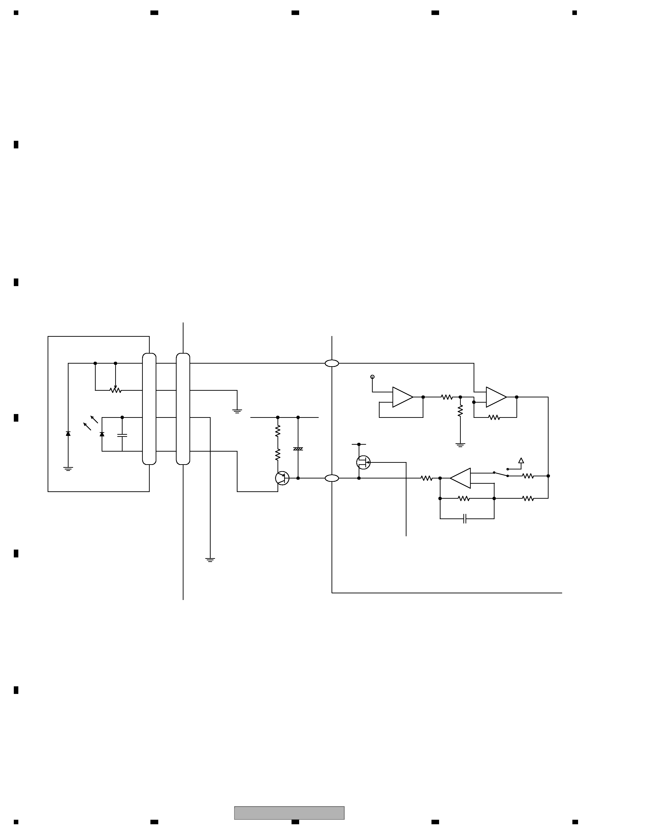
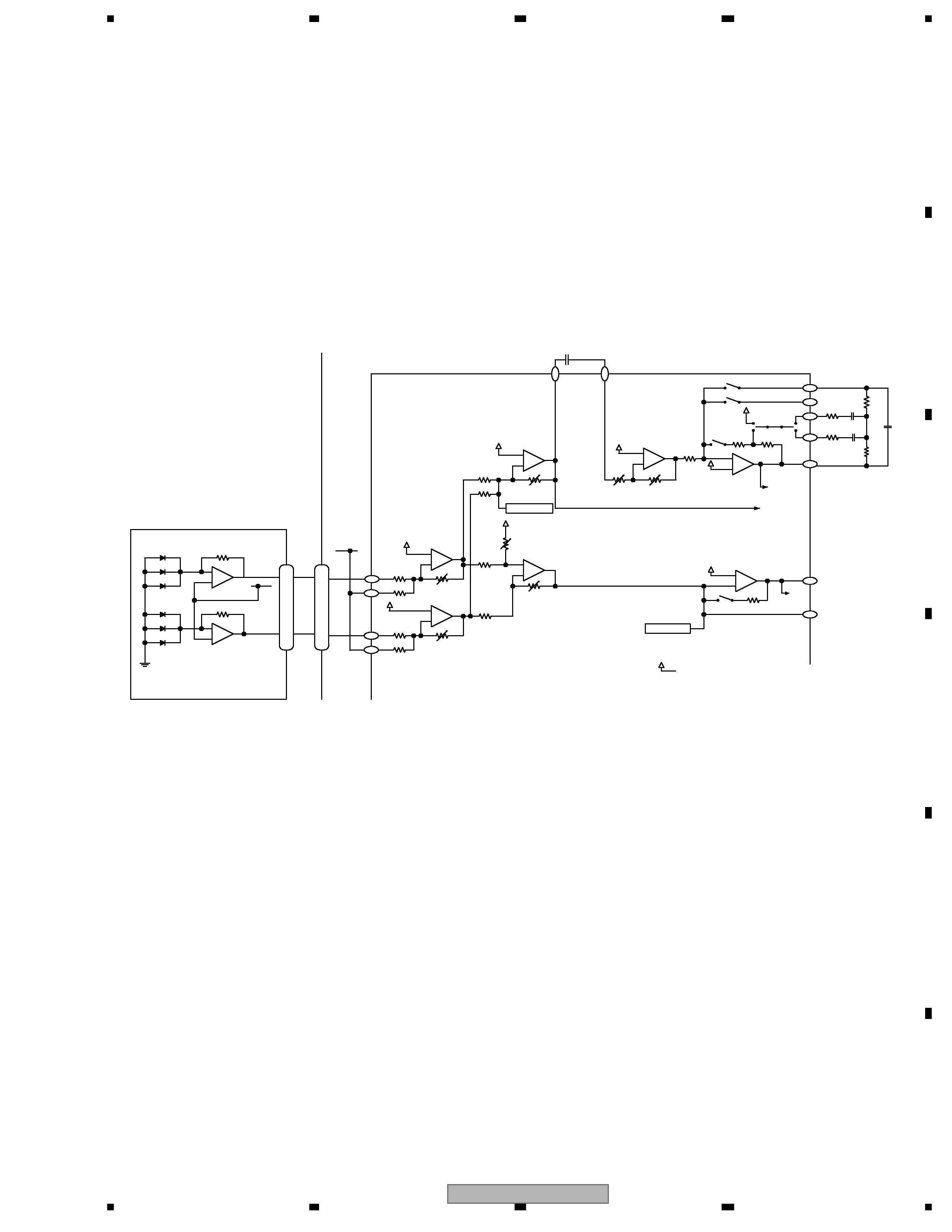
In the preamplifier block, the pickup output signals are processed to generate signals that are used in the subsequent
blocks: servo, demodulator, and control blocks. Signals from the pickup are I/V converted in the pickup with the
preamplifier with built-in photo detectors, and after added with the RF amplifier, they are used to produce such signals as
RF, FE, TE, and TE zero-cross signals. The preamplifier block is built in CD LSI UPD63763CGJ (IC201), whose parts are
described individually below. Incidentally, as this LSI employs a single power supply (+ 3.3 V) specification, the reference
voltages of this LSI and the pickup are the REFO (1.65 V) for both. The REFO is an output obtained from REFOUT in the
LSI via the buffer amplifier, and is output from the pin 133 of this LSI. All measurements will be performed with this REFO
as the reference.
Caution: Be careful not to short-circuit the REFO and GND when measuring.
1.1.1 APC (Automatic Power Control) circuit
Since laser diodes have extremely negative temperature characteristics in optical output when driven in constant current,
it is necessary to control the current with the monitor diodes in order to keep the output constant. This is the feature of the
APC circuit. The LD current is obtained by measuring the voltage between LD1 and V3R3D(+ 3.3 V), and divide the value
by 7.5 (ohms), which becomes about 30 mA.
Fig.1.1.1 APC
1.1 PREAMPLIFIER BLOCK (UPD63763CGJ: IC201)
background image
CX-3164
5
56
7
8
56
7
8
C
D
F
A
B
E
13
6
A+C
B+C
VREF
13
6
10k
10k
8.8k
10k
10k
8.8k
61.0k
61.0k
111k
R2
15.2k
15.2k
35k
20k
11.2k
7.05k
10k
10k
124
127
125
126
122
120
121
116
136
135
RFOFF setup
FEOFF setup
VREF
VREF
A
B
C
D
RFO
AGCI
RF2-
RF-
EQ2
EQ1
AGCO
FEO
FE-
FE A/D
118
119
+
-
+
-
+
-
+
-
+
-
+
-
-
+
P3
P7
P9
P2
P4
P8
Pickup Unit
CD CORE UNIT
UPD63763CGJ
4.7k
5.6k
1.2k
1.2k
22p
56p
4p
123
For RFOK generation
To DEFECT/A3T detection
1.1.2 RF and RFAGC amplifiers
The output from the photo-detector (A + C) and (B + D) is provided from the RFO terminal as the RF signal (which can be
used for eye-pattern check), after it is added, amplified, and equalized inside this LSI. The low frequency component of
the voltage RFO is calculated as below.
RFO = (A + B + C + D) x 2
The RFO is used for the FOK generation circuit and RF offset adjustment circuit.
The RFO signal, output from the pin 119, is A/C-coupled externally, input to the pin 118, and amplified in the RFAGC
amplifier to obtain the RFAGC signal.
Also, this LSI is equipped with the RFAGC auto-adjustment function, explained below, which switches feedback gains of
the RFAGC amplifier so that the RFO output will be 1.5 V.
This RFO signal is also used for the EFM, DFCT, MIRR, and RFAGC auto-adjustment circuits.
Fig.1.1.2 RF/AGC/FE

Reviews

There are no reviews of this manual yet.