SERVICE MANUAL
3
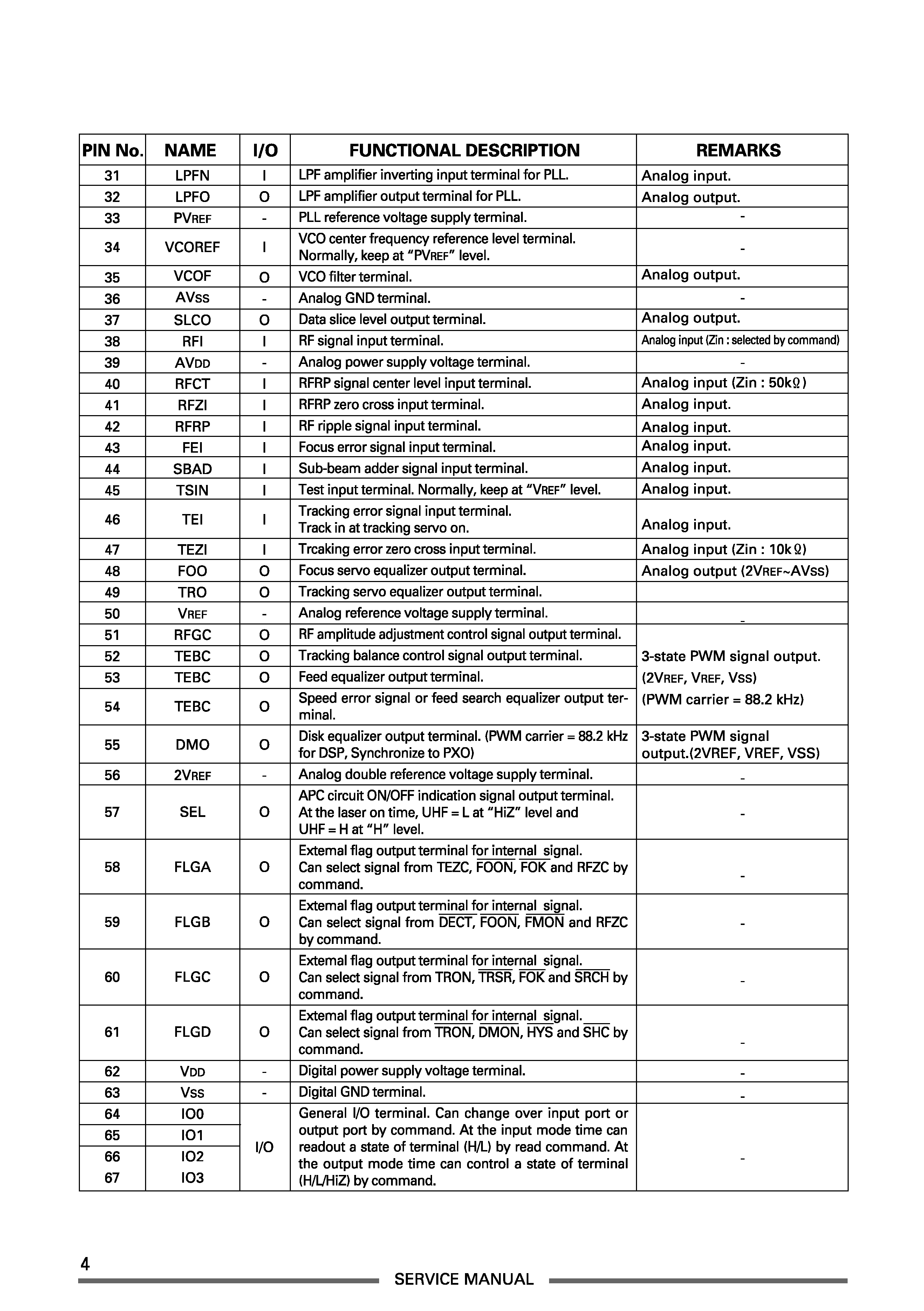
TC9432AF/ TC9462AF (Digital Signal Processor)
PIN No. NAME
I/O
FUNCTIONAL DESCRIPTION
REMARKS
TEST0
HSO
UHSO
EMPH
LRCK
VSS
BCK
AOUT
DOUT
MBOV
IPF
SBOK
CLCK
VDD
VSS
DATA
SFSY
SBSY
SPCK
SPDA
COFS
MONIT
VDD
TESIO0
P2VREF
HSSW
ZDET
PDO
TMAXS
TMAX
With pull-up resistor.
-
-
-
-
-
-
-
-
-
-
-
-
-
-
-
-
-
-
-
-
-
-
-
2-state output (PVREF,HiZ)
-
3-state output
(P2VREF,PVREF,VSS)
-
3-state output
(P2VREF,HiZ,VSS)
1
2
3
4
5
6
7
8
9
10
11
12
13
14
15
16
17
18
19
20
21
22
23
24
25
26
27
28
29
30
Test mode terminal. Normally, keep at open.
Playback speed mode flag output terminal.
Subcode Q data emphasis flag output terminal.
Emphasis ON at "H" level and OFF at "L" level.
The output polarity can invert by command.
Channel clock output terminal. (44.1 kHz)
L-ch at "L" level and R-ch at "H" level.
The output polarity can invert by command.
Digital GND terminal.
Bit clock output terminal. (1.4112 MHz)
Audio data output terminal.
Digital data output terminal.
Buffer memory over signal output terminal.
Over at "H" level.
Correction flag output terminal.
At "H " level, AOUT output is made to correction
impossibility by C2 correction processing.
Subcode Q data CRCC check adjusting result output
terminal. The adjusting result is OK at "H" level.
Subcode P~W data readout clock input/output termi-
nal. This terminal can select by command bit.
Digital power supply voltage terminal.
Digital GND terminal.
Subcode P~W data output terminal.
Playback frame sync signal output terminal.
Subcode block sync signal output terminal.
Processor status signal readout clock output terminal.
Processor status signal output terminal.
Correction frame clock output terminal. (7.35 kHz)
Internal signal (DSP internal flag and PLL clock) output
terminal. Selected by command.
Digital power supply voltage terminal.
Test input/output terminal. Normally, keep at "L" level.
PLL double reference voltage supply terminal.
2/4 times speed at "VREF" voltage.
1 bit DA converter zero detect flag output terminal.
Phase difference signal output terminal of EFM signal
and PLCK signal.
TMAX detection result output terminal. Selected by
command bit (TMPS).
TMAX detection result output terminal. Selected by
command bit (TMPS).
-
O
O
O
O
-
O
O
O
O
O
O
I/O
-
-
O
O
O
O
O
O
O
-
I
-
O
O
O
O
O
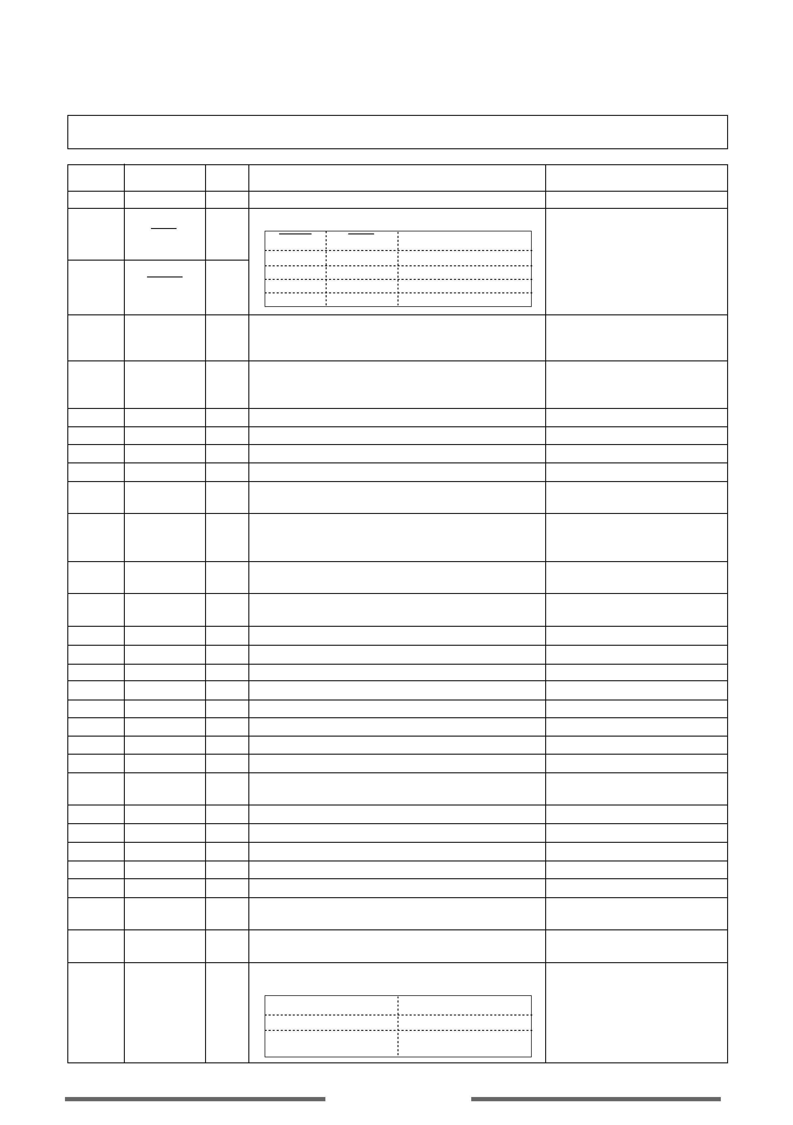
UHSO
HSO
PLAYBACK SPEED
H
H
Normal
H
L
2 times
L
H
4 times
L
L
-
DIFFERENCE RESULT
TMAX OUTPUT
Longer than fixed ferq.
"P2VREF"
Shorter than fixed freq.
"VSS"
Within the fixed freq.
"HiZ"