PIONEER XR-A100/NVXK Service Manual

Cover page of PIONEER XR-A100/NVXK Service Manual

Service Manual for PIONEER XR-A100/NVXK, downloadable as a PDF file.

Manual details

  • Immediate download after payment.
  • Delivered as a PDF file.
  • The manual has 28 pages
  • File size: 2.6 MB
  • Available language versions: English
  • Different language versions may vary sligthly in file size and page count.

We guarantee that...

  • our manuals are complete,
  • the manual includes circuit diagrams,
  • our manuals are checked with antivirus,
  • We'll issue refund if the manual is damaged, incomplete or unreadable (our refund policy)

Sample pages

Thumbnail of page 1Thumbnail of page 2Thumbnail of page 3Thumbnail of page 4
Thumbnail of page 5Thumbnail of page 6Thumbnail of page 7Thumbnail of page 8
Thumbnail of page 9
background image
ORDER NO.
PIONEER ELECTRONIC CORPORATION 4-1, Meguro 1-Chome, Meguro-ku, Tokyo 153-8654, Japan
PIONEER ELECTRONICS SERVICE, INC. P.O. Box 1760, Long Beach, CA 90801-1760, U.S.A.
PIONEER ELECTRONIC (EUROPE) N.V. Haven 1087, Keetberglaan 1, 9120 Melsele, Belgium
PIONEER ELECTRONICS ASIACENTRE PTE. LTD. 501 Orchard Road, #10-00 Lane Crawford Place, Singapore 0923
PIONEER ELECTRONIC CORPORATION 1998
XR-A100-K
XR-A100
RRV1916
1. SAFETY INFORMATION ...................................... 2
2. CONTRAST OF MISCELLANEOUS PARTS ........ 3
3. SCHEMATIC DIAGRAM ..................................... 10
4. PCB CONNECTION DIAGRAM .......................... 19
5. ADJUSTMENT .................................................... 27
CONTENTS
T ­ DZK FEB. 1998 Printed in Japan
Refer to the service manual RRV1883 for XR-A100-K/KCXJ .
STEREO CD CASSETTE DECK RECEIVER
MYXK
AC220­230V
NVXK
AC230V
YPWXJ
­­
AC240V
THIS MANUAL IS APPLICABLE TO THE FOLLOWING MODEL(S) AND TYPE(S).
Model
XR-A100
XR-A100-K
Type
Power Requirement
Remarks
background image
XR-A100, XR-A100-K
2
Name Label
1. SAFETY INFORMATION
This service manual is intended for qualified service technicians; it is not meant for the casual
do-it-yourselfer. Qualified technicians have the necessary test equipment and tools, and have been
trained to properly and safely repair complex products such as those covered by this manual.
Improperly performed repairs can adversely affect the safety and reliability of the product and may
void the warranty. If you are not qualified to perform the repair of this product properly and safely, you
should not risk trying to do so and refer the repair to a qualified service technician.
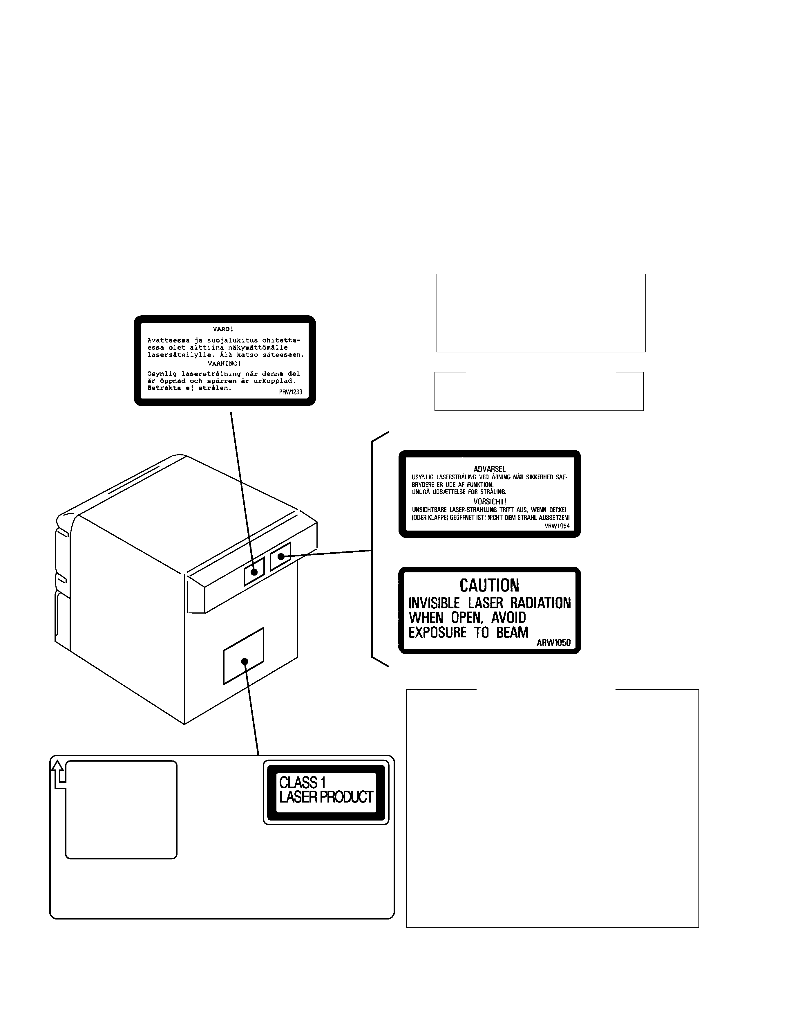
LABEL CHECK
IMPORTANT
THIS PIONEER APPARATUS CONTAINS
LASER OF CLASS 1.
SERVICING OPERATION OF THE APPARATUS
SHOULD BE DONE BY A SPECIALLY
INSTRUTED PERSON.
LASER DIODE CHARACTERISTICS
MAXIMUM OUTPUT POWER: 5 mw
WAVELENGTH: 780 ­ 785 nm
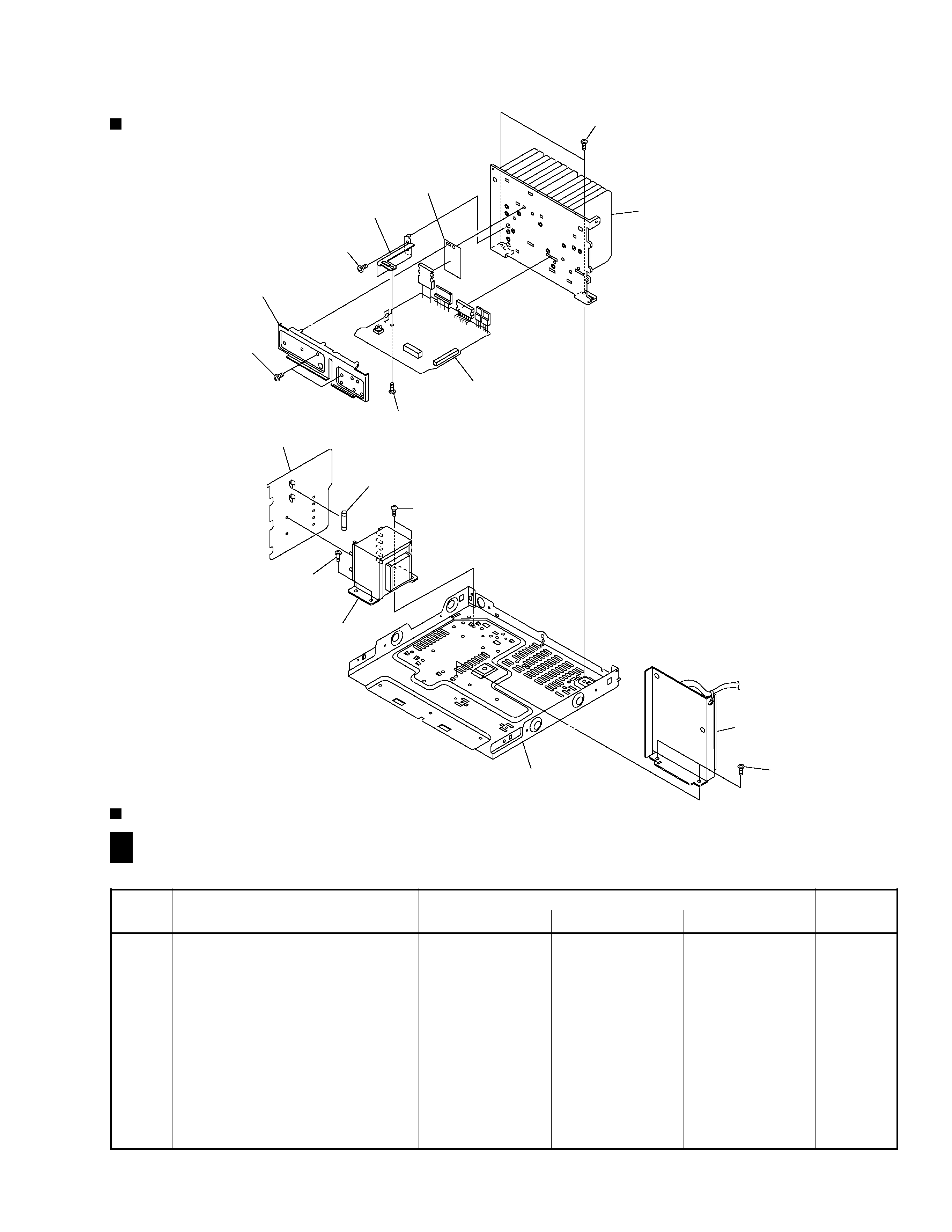
Additional Laser Caution
1. Laser Interlock Mechanism
The position of the switch (S8501) for detecting loading
state is detected by the system microprocessor, and
the design prevents laser diode oscillation when the
switch (S8501) is pressed physically.
Thus, the interlock will no longer function if the switch (S8501)
is released physically and deliberatery.
The interlock also does not function in the test mode
.
Laser diode oscillation will continue, if pin 62 of
LA9240ML (IC8101) on the CD ASSY mounted on the
$M Loading Mechanism assembly is connected to GND,
or else the terminals of Q8101 are shorted to each other
(fault condition).
2. When the cover is opened, close viewing of the
objective lens with the naked eye will cause exposure
to a Class 1 laser beam.
: Refer to page 52 on the service manual RRV1883.
MYXK Type
MYXK, NVXK and YPWXJ Types
MYXK Type
NVXK Type
background image
XR-A100, XR-A100-K
3
.
f
e
R
.
o
N
k
r
a
Mn
o
i
t
p
i
r
c
s
e
D
d
n
a
l
o
b
m
y
S
.
o
N
t
r
a
P
s
k
r
a
m
e
R
K
-
0
0
1
A
-
R
X
J
X
C
K
/
0
0
1
A
-
R
X
K
X
Y
M
/
0
0
1
A
-
R
X
K
X
V
N
/
0
0
1
A
-
R
X
J
X
W
P
Y
/
K
-
0
0
1
A
-
R
X
K
X
Y
M
/
K
-
0
0
1
A
-
R
X
K
X
V
N
/
1
-
7
P
y
s
s
A
F
A4
0
0
3
M
W
X7
0
0
3
M
W
X7
0
0
3
M
W
X1
0
0
3
M
W
X7
0
0
3
M
W
X7
0
0
3
M
W
X
*1
P
S
Ny
s
s
A
Y
L
P
P
U
S
R
E
W
O
P5
0
0
3
M
W
X0
6
2
7
M
W
A0
6
2
7
M
W
A3
8
2
7
M
W
A0
6
2
7
M
W
A0
6
2
7
M
W
A
2
-
7
P
y
s
s
A
S
N
A
R
T0
1
0
3
Z
W
X7
4
5
8
Z
W
A7
4
5
8
Z
W
A8
3
5
8
Z
W
A7
4
5
8
Z
W
A7
4
5
8
Z
W
A
*1
3
-
7
P
y
s
s
A
R
E
W
O
P1
1
0
3
Z
W
X8
4
5
8
Z
W
A8
4
5
8
Z
W
A4
3
5
8
Z
W
A8
4
5
8
Z
W
A8
4
5
8
Z
W
A
*1
9
2
-
7
P
2
y
s
s
A
R
E
W
O
P2
1
0
3
Z
W
Xd
e
s
u
t
o
Nd
e
s
u
t
o
Nd
e
s
u
t
o
Nd
e
s
u
t
o
Nd
e
s
u
t
o
N
0
3
-
7
P
y
s
s
A
2
S
N
A
R
T3
1
0
3
Z
W
Xd
e
s
u
t
o
Nd
e
s
u
t
o
Nd
e
s
u
t
o
Nd
e
s
u
t
o
Nd
e
s
u
t
o
N
P
S
Ny
s
s
A
X
E
L
P
M
O
C6
0
0
3
M
W
X8
0
0
3
M
W
X8
0
0
3
M
W
X2
0
0
3
M
W
X8
0
0
3
M
W
X8
0
0
3
M
W
X
1
-
9
P
y
s
s
A
K
C
E
D7
0
0
3
Z
W
X7
1
0
3
Z
W
X7
1
0
3
Z
W
X2
0
0
3
Z
W
X7
1
0
3
Z
W
X7
1
0
3
Z
W
X
4
-
9
P
y
s
s
A
Y
A
L
P
S
I
D4
1
0
3
Z
W
X6
1
0
3
Z
W
X6
1
0
3
Z
W
X1
0
0
3
Z
W
X6
1
0
3
Z
W
X6
1
0
3
Z
W
X
5
-
9
P
y
s
s
A
D
C
L5
1
0
3
Z
W
X8
1
0
3
Z
W
X8
1
0
3
Z
W
X6
0
0
3
Z
W
X8
1
0
3
Z
W
X8
1
0
3
Z
W
X
6
-
9
P
y
s
s
A
P
M
A
L8
0
0
3
Z
W
X4
2
0
3
Z
W
X4
2
0
3
Z
W
X8
0
0
3
Z
W
X4
2
0
3
Z
W
X4
2
0
3
Z
W
X
4
-
7
P
E
L
U
D
O
M
R
E
N
U
T
M
A
/
M
F1
6
0
7
Q
X
A
7
7
0
7
Q
X
A
*2
7
7
0
7
Q
X
A
*2
1
6
0
7
Q
X
A
7
7
0
7
Q
X
A
*2
7
7
0
7
Q
X
A
*2
1
-
3
Pa
n
n
e
t
n
A
M
F4
0
0
7
H
D
A5
0
0
7
H
D
A5
0
0
7
H
D
A4
0
0
7
H
D
A5
0
0
7
H
D
A5
0
0
7
H
D
A
2
-
3
Ps
n
o
i
t
c
u
r
t
s
n
I
g
n
i
t
a
r
e
p
O5
0
0
3
E
R
Xd
e
s
u
t
o
Nd
e
s
u
t
o
N5
0
0
3
E
R
Xd
e
s
u
t
o
Nd
e
s
u
t
o
N
)
h
s
i
n
a
p
S
/
h
c
n
e
r
F
/
h
s
il
g
n
E
(
s
n
o
i
t
c
u
r
t
s
n
I
g
n
i
t
a
r
e
p
Od
e
s
u
t
o
N1
0
0
3
C
R
Xd
e
s
u
t
o
Nd
e
s
u
t
o
N1
0
0
3
C
R
Xd
e
s
u
t
o
N
)
h
c
t
u
D
/
n
a
m
r
e
G
/
h
c
n
e
r
F
(
s
n
o
i
t
c
u
r
t
s
n
I
g
n
i
t
a
r
e
p
Od
e
s
u
t
o
N2
0
0
3
C
R
Xd
e
s
u
t
o
Nd
e
s
u
t
o
N2
0
0
3
C
R
Xd
e
s
u
t
o
N
)
n
a
i
s
s
u
R
/
h
s
i
d
e
w
S
/
n
a
il
a
t
I
(
s
n
o
i
t
c
u
r
t
s
n
I
g
n
i
t
a
r
e
p
Od
e
s
u
t
o
N6
0
0
3
E
R
Xd
e
s
u
t
o
Nd
e
s
u
t
o
N6
0
0
3
E
R
Xd
e
s
u
t
o
N
)
e
s
e
u
g
u
t
r
o
P
/
h
s
i
n
a
p
S
/
h
s
il
g
n
E
(
)
h
s
il
g
n
E
(
s
n
o
i
t
c
u
r
t
s
n
I
g
n
i
t
a
r
e
p
Od
e
s
u
t
o
Nd
e
s
u
t
o
N1
0
0
3
B
R
Xd
e
s
u
t
o
Nd
e
s
u
t
o
N1
0
0
3
B
R
X
3
-
3
Pa
n
n
e
t
n
A
p
o
o
L
M
A1
0
0
3
B
T
X7
0
0
7
B
T
A7
0
0
7
B
T
A1
0
0
3
B
T
X7
0
0
7
B
T
A7
0
0
7
B
T
A
4
-
3
Pt
i
n
U
l
o
r
t
n
o
C
e
t
o
m
e
R2
0
0
3
N
Z
X2
0
0
3
N
Z
X2
0
0
3
N
Z
Xd
e
s
u
t
o
N2
0
0
3
N
Z
X2
0
0
3
N
Z
X
)
0
4
0
R
X
-
U
C
(
4
-
3
Pt
i
n
U
l
o
r
t
n
o
C
e
t
o
m
e
Rd
e
s
u
t
o
Nd
e
s
u
t
o
Nd
e
s
u
t
o
N3
0
0
3
N
Z
Xd
e
s
u
t
o
Nd
e
s
u
t
o
N
)
9
3
0
R
X
-
U
C
(
0
1
-
3
Pe
s
a
C
g
n
i
k
c
a
P8
0
0
3
D
H
X0
1
0
3
D
H
X0
1
0
3
D
H
X7
0
0
3
D
H
X1
3
0
3
D
H
X1
3
0
3
D
H
X
1
1
-
3
Pt
e
e
h
S
g
n
i
k
c
a
P3
0
0
7
G
H
A1
0
0
7
G
H
A1
0
0
7
G
H
A3
0
0
7
G
H
A1
0
0
7
G
H
A1
0
0
7
G
H
A
2. CONTRAST OF MISCELLANEOUS PARTS
CONTRAST TABLE
XR-A100/MYXK, NVXK, YPWXJ, XR-A100-K/MYXK, NVXK and XR-A100-K/KCXJ are constructed the same
except for the following :
NOTES:
·Parts marked by "NSP" and can not be supplied.
·The mark found on some component parts indicates the importance of the safety factor of the part.
Therefore, when replacing, be sure to use parts of identical designation.
·When ordering resistors, first convert resistance values into code form as shown in the following examples.
Ex.1 When there are 2 effective digits (any digit apart from 0), such as 560 ohm and 47k ohm (tolerance is shown by J=5%,
and K=10%).
560
56
× 101
561 ........................................................ RD1/4PU 5 6 1 J
47k
47
× 103
473 ........................................................ RD1/4PU 4 7 3 J
0.5
R50 ..................................................................................... RN2H R 5 0 K
1
1R0 ..................................................................................... RS1P 1 R 0 K
Ex.2 When there are 3 effective digits (such as in high precision metal film resistors).
5.62k
562
× 101
5621 ...................................................... RN1/4PC 5 6 2 1 F
·Reference Nos. indicate the pages and Nos. in the service manual for the base model.
Notes *1 : Refer to "PCB PARTS LIST" , "3. SCHEMATIC DIAGRAM" and "4. PCB CONNECTION DIAGRAM".
*2 : Refer to "PCB PARTS LIST" , "3. SCHEMATIC DIAGRAM" , "4. PCB CONNECTION DIAGRAM" and "5. ADJUSTMENT".
background image
XR-A100, XR-A100-K
4
.
f
e
R
.
o
N
k
r
a
Mn
o
i
t
p
i
r
c
s
e
D
d
n
a
l
o
b
m
y
S
.
o
N
t
r
a
P
s
k
r
a
m
e
R
K
-
0
0
1
A
-
R
X
J
X
C
K
/
0
0
1
A
-
R
X
K
X
Y
M
/
0
0
1
A
-
R
X
K
X
V
N
/
0
0
1
A
-
R
X
J
X
W
P
Y
/
K
-
0
0
1
A
-
R
X
K
X
Y
M
/
K
-
0
0
1
A
-
R
X
K
X
V
N
/
2
1
-
3
PP
S
Nd
r
a
C
y
t
n
a
r
r
a
W5
7
0
1
Y
R
A0
1
0
7
Y
R
A0
1
0
7
Y
R
A3
0
0
1
Y
R
P0
1
0
7
Y
R
A0
1
0
7
Y
R
A
6
-
5
Pp
a
C
y
a
r
T6
1
0
3
K
A
X8
0
0
3
K
A
X8
0
0
3
K
A
X8
0
0
3
K
A
X6
1
0
3
K
A
X6
1
0
3
K
A
X
7
-
5
Pl
e
n
a
P
y
a
l
p
s
i
D5
0
0
3
K
A
X5
0
0
3
K
A
X5
0
0
3
K
A
X3
0
0
3
K
A
X5
0
0
3
K
A
X5
0
0
3
K
A
X
8
-
5
Pe
s
a
C
t
e
n
n
o
B5
0
0
3
N
Z
X1
0
0
3
N
Z
X1
0
0
3
N
Z
X1
0
0
3
N
Z
X5
0
0
3
N
Z
X5
0
0
3
N
Z
X
3
1
-
5
PP
S
Nl
e
b
a
L
5
6
&
P
C
I1
2
5
7
X
A
Ad
e
s
u
t
o
Nd
e
s
u
t
o
Nd
e
s
u
t
o
Nd
e
s
u
t
o
Nd
e
s
u
t
o
N
1
3
-
7
Pr
e
i
r
r
a
B
C
V
P4
7
0
7
C
E
A9
2
0
7
K
N
A9
2
0
7
K
N
A9
2
0
7
K
N
A9
2
0
7
K
N
A9
2
0
7
K
N
A
5
-
7
P)
V
0
2
1
C
A
(
r
e
m
r
o
f
s
n
a
r
T
r
e
w
o
P4
0
0
3
S
T
Xd
e
s
u
t
o
Nd
e
s
u
t
o
Nd
e
s
u
t
o
Nd
e
s
u
t
o
Nd
e
s
u
t
o
N
5
-
7
Pr
e
m
r
o
f
s
n
a
r
T
r
e
w
o
Pd
e
s
u
t
o
N2
4
1
7
S
T
A2
4
1
7
S
T
Ad
e
s
u
t
o
N2
4
1
7
S
T
A2
4
1
7
S
T
A
)
V
0
3
2
-
0
2
2
C
A
(
5
-
7
P)
V
0
4
2
C
A
(
r
e
m
r
o
f
s
n
a
r
T
r
e
w
o
Pd
e
s
u
t
o
Nd
e
s
u
t
o
Nd
e
s
u
t
o
N9
3
1
7
S
T
Ad
e
s
u
t
o
Nd
e
s
u
t
o
N
6
-
7
P)
1
U
F
,
A
5
1
.
3
(
e
s
u
F1
8
0
1
K
E
Rd
e
s
u
t
o
Nd
e
s
u
t
o
Nd
e
s
u
t
o
Nd
e
s
u
t
o
Nd
e
s
u
t
o
N
6
-
7
P)
1
U
F
,
A
1
T
(
e
s
u
Fd
e
s
u
t
o
N4
5
0
1
K
E
A4
5
0
1
K
E
Ad
e
s
u
t
o
N4
5
0
1
K
E
A4
5
0
1
K
E
A
6
-
7
P)
1
U
F
,
A
1
(
e
s
u
Fd
e
s
u
t
o
Nd
e
s
u
t
o
Nd
e
s
u
t
o
N2
2
0
1
K
E
Rd
e
s
u
t
o
Nd
e
s
u
t
o
N
7
-
7
Pd
r
o
C
r
e
w
o
P
C
A7
5
0
1
G
D
P8
0
0
7
G
D
A7
0
0
7
G
D
A9
5
1
1
G
D
A8
0
0
7
G
D
A7
0
0
7
G
D
A
)
g
u
l
P
C
A
n
i
h
t
i
W
(
)
A
5
T
(
e
s
u
Fd
e
s
u
t
o
Nd
e
s
u
t
o
N1
0
0
7
K
E
Ad
e
s
u
t
o
Nd
e
s
u
t
o
N1
0
0
7
K
E
A
0
1
-
7
Pe
t
a
l
P
D
N
G6
0
1
7
G
N
A1
3
1
7
G
N
A1
3
1
7
G
N
A6
0
1
7
G
N
A1
3
1
7
G
N
A1
3
1
7
G
N
A
2
1
-
7
Pe
t
a
l
P
d
l
e
i
h
S2
3
1
7
G
N
A8
1
1
7
G
N
A8
1
1
7
G
N
A8
1
1
7
G
N
A8
1
1
7
G
N
A8
1
1
7
G
N
A
3
1
-
7
Pk
n
i
S
t
a
e
H3
6
0
7
H
N
A7
4
0
7
H
N
A7
4
0
7
H
N
A9
5
0
7
H
N
A7
4
0
7
H
N
A7
4
0
7
H
N
A
5
1
-
7
Pr
e
v
o
C
r
a
e
R1
1
0
7
C
M
A3
0
0
7
C
M
A3
0
0
7
C
M
A3
0
0
7
C
M
A3
0
0
7
C
M
A3
0
0
7
C
M
A
6
1
-
7
Pf
e
il
e
R
n
i
a
r
t
SC
2
2
-
M
CB
2
2
-
M
CB
2
2
-
M
CB
2
2
-
M
CB
2
2
-
M
CB
2
2
-
M
C
6
2
-
7
PP
S
Nl
e
b
a
L
e
m
a
N9
0
0
3
X
A
X2
1
0
3
X
A
X1
1
0
3
X
A
X8
0
0
3
X
A
X2
6
0
3
X
A
X4
6
0
3
X
A
X
8
2
-
7
PC
t
e
k
c
a
r
B7
2
1
7
G
N
Ad
e
s
u
t
o
Nd
e
s
u
t
o
Nd
e
s
u
t
o
Nd
e
s
u
t
o
Nd
e
s
u
t
o
N
3
2
-
9
PP
S
Ny
s
s
A
l
e
n
a
P
t
n
o
r
F8
0
0
3
G
X
X6
0
0
3
G
X
X6
0
0
3
G
X
X2
0
0
3
G
X
X0
1
0
3
G
X
X0
1
0
3
G
X
X
4
2
-
9
Pn
o
t
t
u
B
n
o
i
t
c
n
u
F4
0
0
3
D
A
X1
0
0
3
D
A
X1
0
0
3
D
A
X1
0
0
3
D
A
X4
0
0
3
D
A
X4
0
0
3
D
A
X
0
3
-
9
PL
t
e
k
c
o
P
r
o
o
D3
0
0
3
N
A
X1
0
0
3
N
A
X1
0
0
3
N
A
X1
0
0
3
N
A
X3
0
0
3
N
A
X3
0
0
3
N
A
X
1
3
-
9
PR
t
e
k
c
o
P
r
o
o
D4
0
0
3
N
A
X2
0
0
3
N
A
X2
0
0
3
N
A
X2
0
0
3
N
A
X4
0
0
3
N
A
X4
0
0
3
N
A
X
2
3
-
9
Pl
e
n
a
P
t
n
o
r
F8
0
0
3
B
M
X6
0
0
3
B
M
X6
0
0
3
B
M
X2
0
0
3
B
M
X0
1
0
3
B
M
X0
1
0
3
B
M
X
B
l
e
b
a
L
C
O
D5
8
6
1
W
R
Dd
e
s
u
t
o
Nd
e
s
u
t
o
Nd
e
s
u
t
o
Nd
e
s
u
t
o
Nd
e
s
u
t
o
N
A
t
e
k
c
a
r
Bd
e
s
u
t
o
N0
0
1
7
G
N
A0
0
1
7
G
N
A0
0
1
7
G
N
A0
0
1
7
G
N
A0
0
1
7
G
N
A
*
1
.
o
N
,
3
)
A
t
e
k
c
a
r
B
r
o
f
(
w
e
r
c
Sd
e
s
u
t
o
N
C
M
F
0
2
1
P
0
3
Z
B
BC
M
F
0
2
1
P
0
3
Z
B
BC
M
F
0
2
1
P
0
3
Z
B
BC
M
F
0
2
1
P
0
3
Z
B
BC
M
F
0
2
1
P
0
3
Z
B
B
*
2
.
o
N
,
3
)
e
t
a
l
P
d
l
e
i
h
S
r
o
f
(
w
e
r
c
Sd
e
s
u
t
o
N
BCZ4
F
0
6
0
P
0K
Z
BCZ4
F
0
6
0
P
0K
Z
BCZ4
F
0
6
0
P
0K
Z
BCZ4
F
0
6
0
P
0K
Z
BCZ4
F
0
6
0
P
0K
Z
*
3
.
o
N
,
3
r
o
t
i
c
a
p
a
C
c
i
m
a
r
e
Cd
e
s
u
t
o
N
0
5
K
2
2
1
B
Y
C
K
C0
5
K
2
2
1
B
Y
C
K
C
d
e
s
u
t
o
N
0
5
K
2
2
1
B
Y
C
K
C0
5
K
2
2
1
B
Y
C
K
C
*4
E
H
l
e
b
a
L
n
o
i
t
u
a
Cd
e
s
u
t
o
N3
3
2
1
W
R
Pd
e
s
u
t
o
Nd
e
s
u
t
o
N3
3
2
1
W
R
Pd
e
s
u
t
o
N
*5
l
e
b
a
L
n
o
i
t
u
a
Cd
e
s
u
t
o
N4
9
0
1
W
R
Vd
e
s
u
t
o
Nd
e
s
u
t
o
N4
9
0
1
W
R
Vd
e
s
u
t
o
N
*5
P
S
Nl
e
b
a
L
n
o
i
t
u
a
Cd
e
s
u
t
o
Nd
e
s
u
t
o
N0
5
0
1
W
R
Ad
e
s
u
t
o
Nd
e
s
u
t
o
N0
5
0
1
W
R
A
*5
b
o
n
K
C
I
Md
e
s
u
t
o
Nd
e
s
u
t
o
Nd
e
s
u
t
o
N1
0
0
3
B
A
Xd
e
s
u
t
o
Nd
e
s
u
t
o
N
*6
Notes *3 : The numbers in the remarks column correspond to the numbers on the "EXPLODED VIEWS".
*4 : Solder to the FM/AM TUNER MODULE and the GND Plate (ANG7131).
*5 : Refer to page 2.
*6 : For MIC LEVEL control (DISPLAY ASSY : VR2501).
background image
XR-A100, XR-A100-K
5
k
r
a
Mn
o
i
t
p
i
r
c
s
e
D
d
n
a
l
o
b
m
y
S
.
o
N
t
r
a
P
s
k
r
a
m
e
R
7
0
0
3
Z
W
X7
1
0
3
Z
W
X2
0
0
3
Z
W
X
1
5
2
4
Ld
e
s
u
t
o
NJ
0
0
1
U
A
Ld
e
s
u
t
o
N
2
2
2
4
C
,
1
2
2
4
C0
5
J
3
7
2
A
B
M
Q
C0
5
J
3
7
2
A
B
M
Q
C0
5
J
3
3
3
A
B
M
Q
C
8
2
2
4
C
,
7
2
2
4
C0
5
K
2
2
2
B
Y
C
K
C0
5
K
2
2
2
B
Y
C
K
C0
5
K
2
5
1
B
Y
C
K
C
5
5
2
4
Cd
e
s
u
t
o
N0
5
K
2
0
1
B
Y
C
K
Cd
e
s
u
t
o
N
7
5
2
4
Cd
e
s
u
t
o
N0
5
M
0
R
1
T
A
E
Cd
e
s
u
t
o
N
3
0
5
4
C
,
1
0
5
4
Cd
e
s
u
t
o
N0
5
J
1
8
1
L
S
D
C
Cd
e
s
u
t
o
N
2
0
5
4
Cd
e
s
u
t
o
N0
5
J
1
8
1
L
S
C
C
Cd
e
s
u
t
o
N
4
0
5
4
Cd
e
s
u
t
o
N0
5
J
1
5
1
L
S
C
C
Cd
e
s
u
t
o
N
2
0
6
4
C
,
1
0
6
4
Cd
e
s
u
t
o
N0
5
J
0
7
4
L
S
C
C
Cd
e
s
u
t
o
N
4
0
6
4
C
,
3
0
6
4
Cd
e
s
u
t
o
N0
5
J
1
0
1
L
S
C
C
Cd
e
s
u
t
o
N
5
0
6
4
Cd
e
s
u
t
o
N0
5
K
2
8
1
B
Y
D
K
Cd
e
s
u
t
o
N
VBZ30P080FZK
VBZ30P080FZK
VBZ30P080FZK
1
2
Fuse (FU1)
Heat Sink
Bracket B
Mica Sheet
POWER ASSY
TRANS ASSY
ABA7031
ABA7031
Power Transformer
Shield Plate
3
Chassis
CONTRAST OF PCB ASSEMBLIES
XWZ3017, XWZ3002 and XWZ3007 are constructed the same except for the following :
DECK ASSY
EXPLODED VIEWS
I F

Reviews

There are no reviews of this manual yet.