ORDER NO.
PIONEER ELECTRONIC CORPORATION 4-1, Meguro 1-Chome, Meguro-ku, Tokyo 153-8654, Japan
PIONEER ELECTRONICS SERVICE, INC. P.O. Box 1760, Long Beach, CA 90801-1760, U.S.A.
PIONEER ELECTRONIC (EUROPE) N.V. Haven 1087, Keetberglaan 1, 9120 Melsele, Belgium
PIONEER ELECTRONICS ASIACENTRE PTE. LTD. 501 Orchard Road, #10-00 Wheelock Place, Singapore 238880
PIONEER ELECTRONIC CORPORATION 1998
RRV2020
T ZZK SEPT. 1998 Printed in Japan
CONTENTS
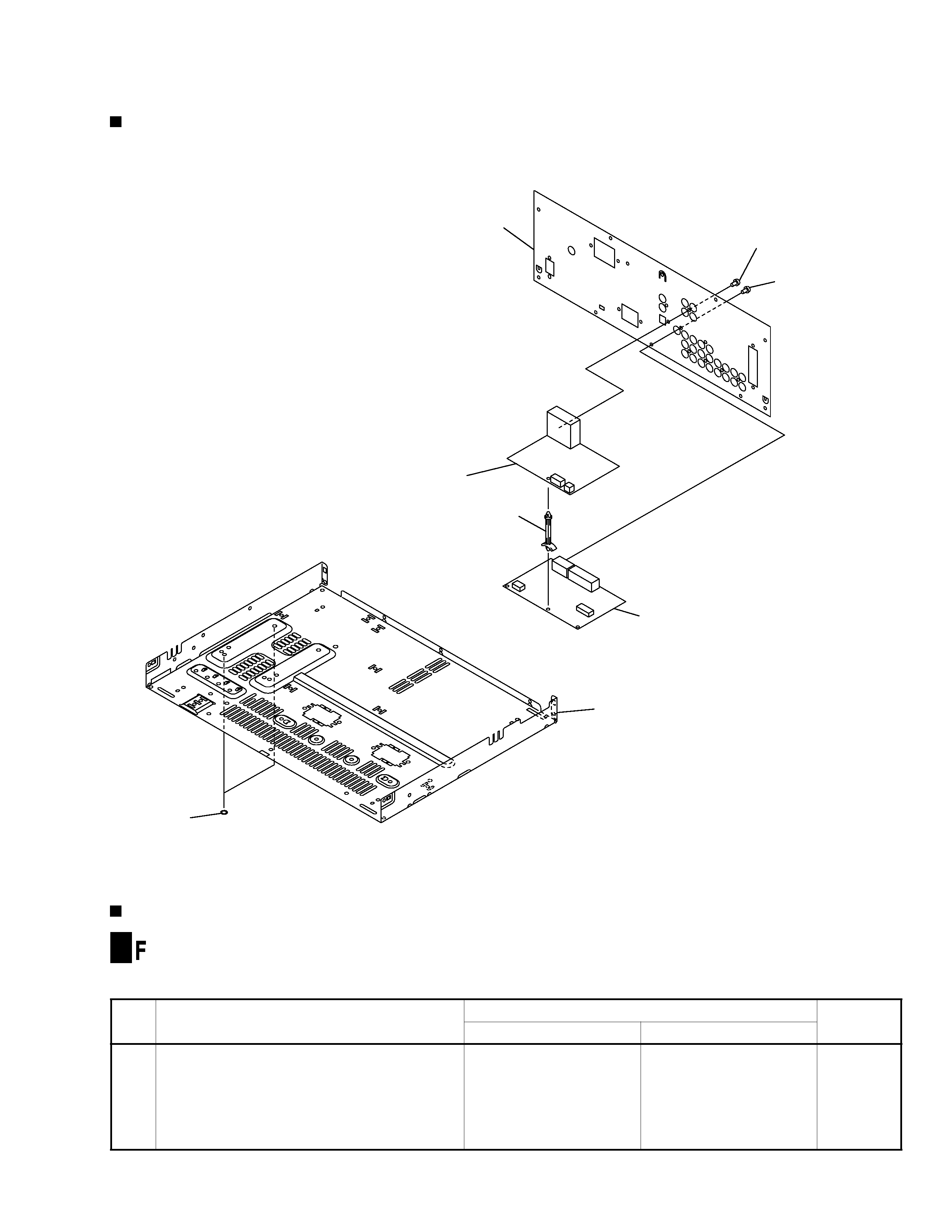
1. CONTRAST OF MISCELLANEOUS PARTS ........ 2
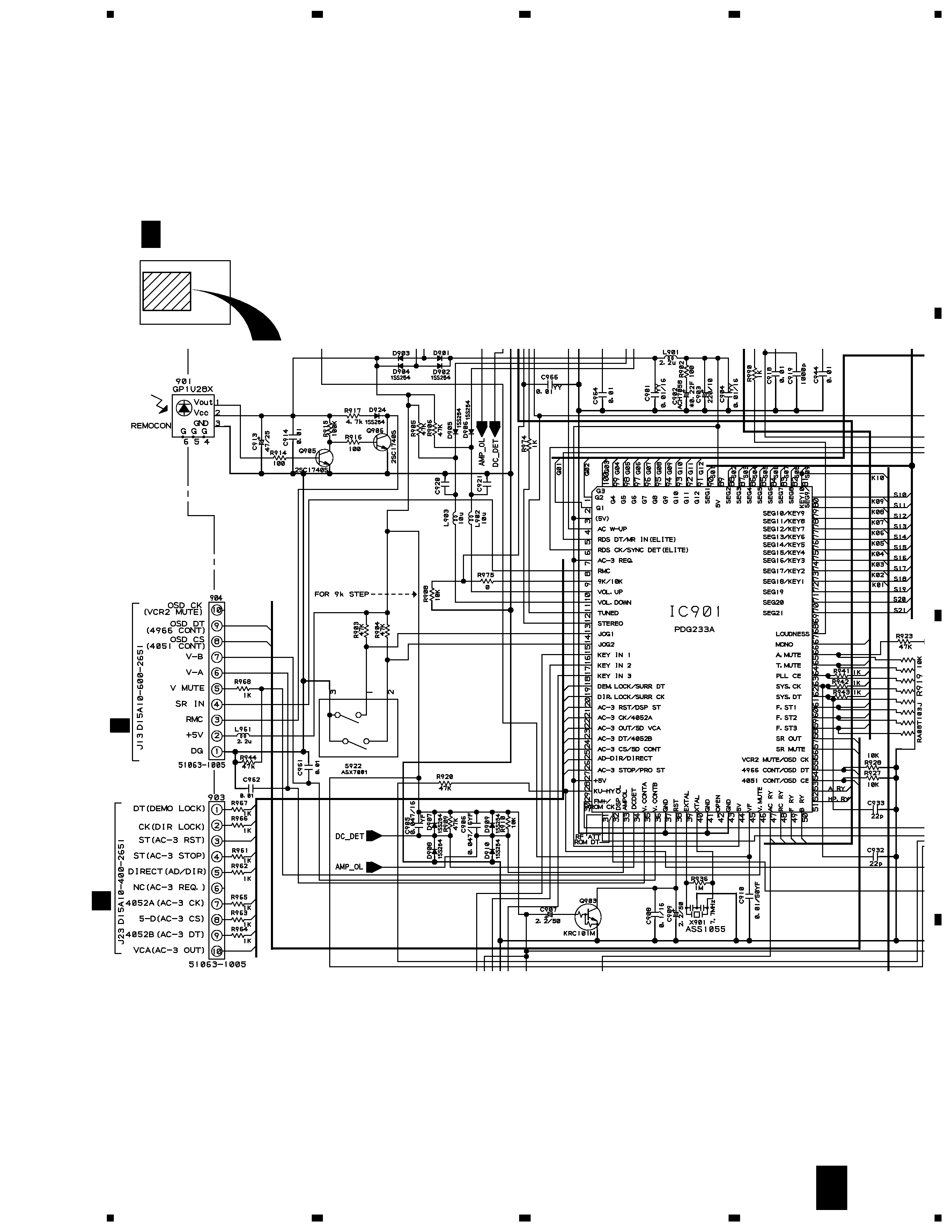
2. SCHEMATIC DIAGRAM ....................................... 5
3. PCB CONNECTION DIAGRAM .......................... 11
¶ Refer to the service manual RRV1769 for VSX-806RDS/HYXJI.
THHYANUAL IS APPLICABLE TO THE FOLLOWING MODEL(S) AND TYPE(S).
Model
VSX-708RDS
Type
Power Requirement
The voltage can be converted by
the following method.
HYXJI
HYXJIGR
AUDIO/VIDEO MULTI-CHANNEL RECEIVER
VSX-708RDS
AC220 230V
AC220 230V
:Alter the wiring of the Power-supply block at the primary winding of Power-transformer referring to the "Line Voltage Selection" described
in Service Manual.
AC240V
AC240V