ORDER NO.
PIONEER CORPORATION 4-1, Meguro 1-chome, Meguro-ku, Tokyo 153-8654, Japan
PIONEER ELECTRONICS SERVICE, INC. P.O. Box 1760, Long Beach, CA 90801-1760, U.S.A.
PIONEER EUROPE N.V. Haven 1087, Keetberglaan 1, 9120 Melsele, Belgium
PIONEER ELECTRONICS ASIACENTRE PTE. LTD. 253 Alexandra Road, #04-01, Singapore 159936
PIONEER CORPORATION 2000
MULTI VIDEO PROCESSOR
ARP3066
TZZB FEB. 2000 Printed in Japan
RMD-V3000X
¶ This service manual should be used together with the following manual(s).
Model No.
Order No.
Remarks
RMD-V3216
ARP2908
RMD-V3070
XGA BOARD
LU/CA
AC100 120V
Z
DC power supplied from other system component
THIS MANUAL IS APPLICABLE TO THE FOLLOWING MODEL(S) AND TYPE(S).
Model
RMD-V3000X
RMD-V3070
Type
Power Requirement
Remarks
1. RMD-V3000X ...................................................... 2
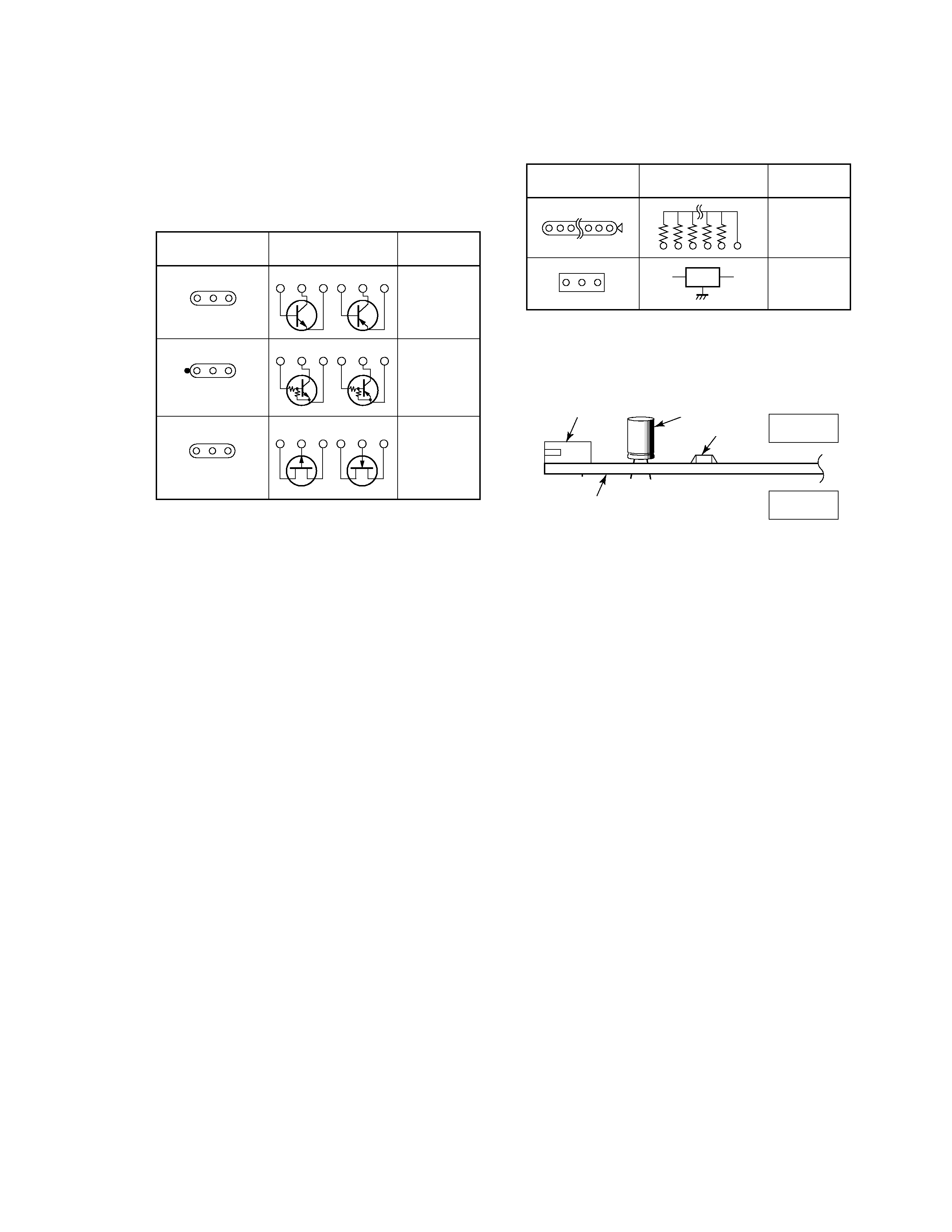
1.1 CONTRAST OF MISCELLANEOUS
PARTS ......................................................... 2
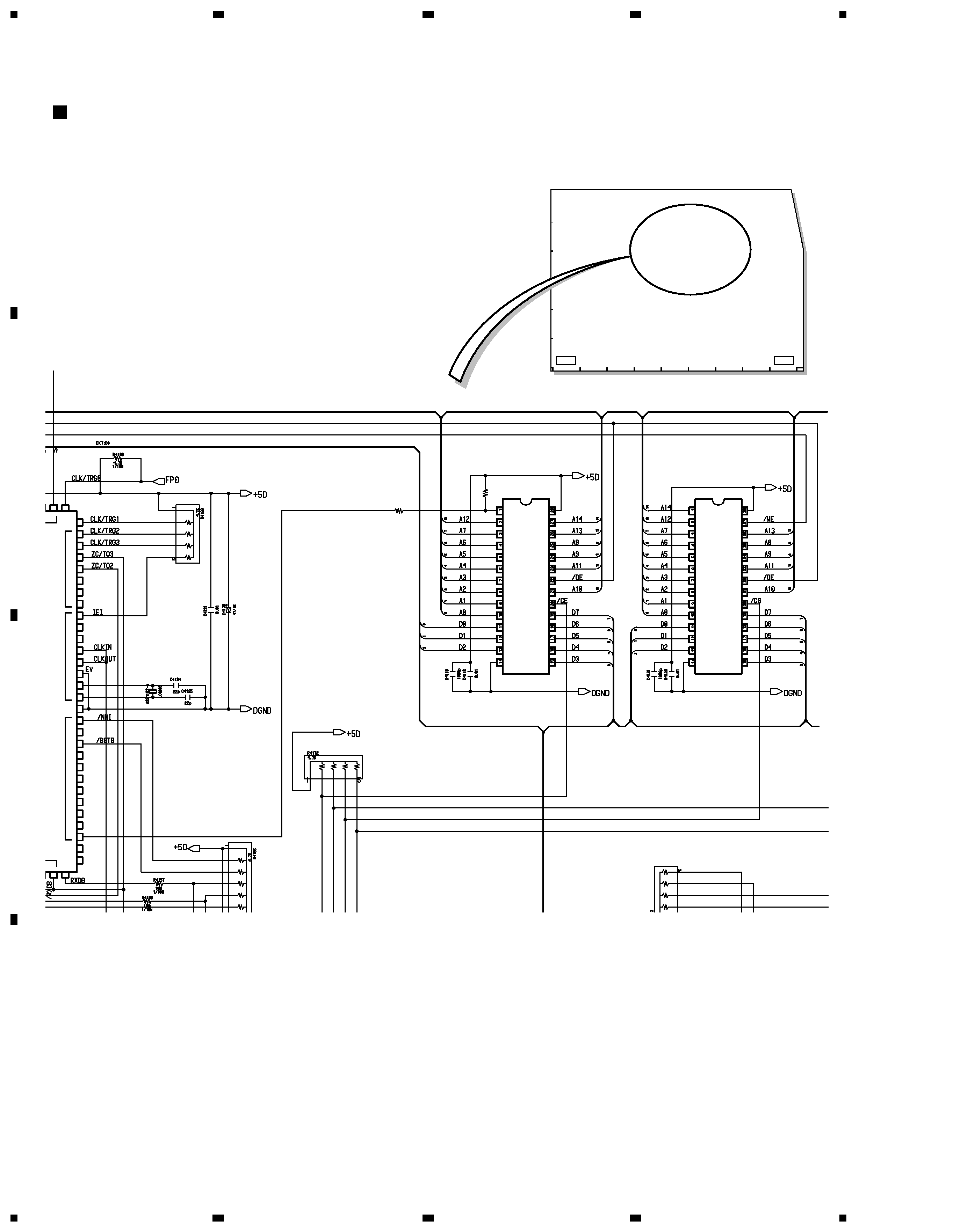
1.2 SCHEMATIC DIAGRAM ............................... 3
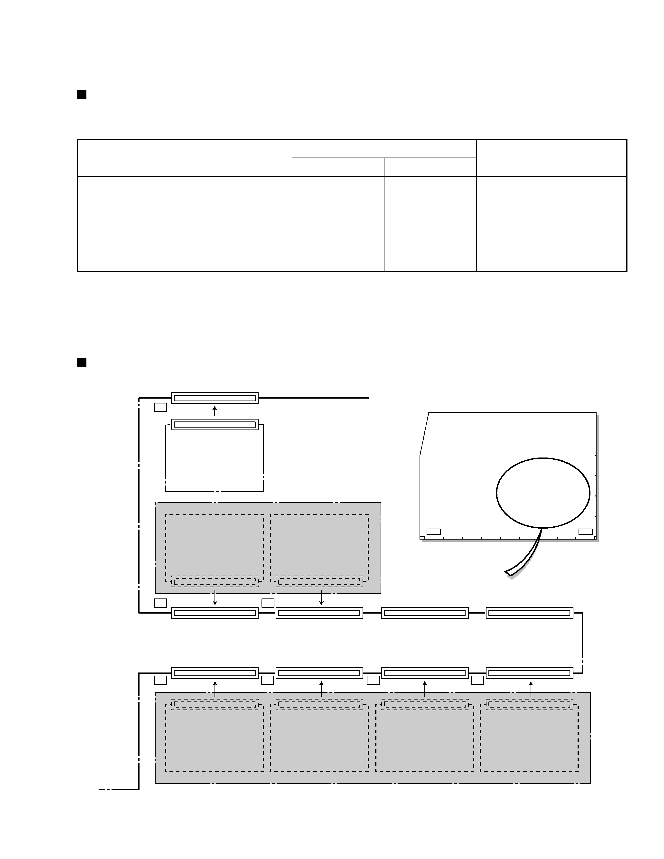
1.3 PCB DIAGRAM ............................................. 5
1.4 GENERAL INFORMATION ........................ 10
2. RMD-V3070 ...................................................... 11
2.1 EXPLODED VIEWS AND PARTS LIST ..... 11
2.2 BLOCK DIAGRAM ...................................... 12
CONTENTS