DVL-919 (1)
2
1. CONTRAST OF MISCELLANEOUS PARTS
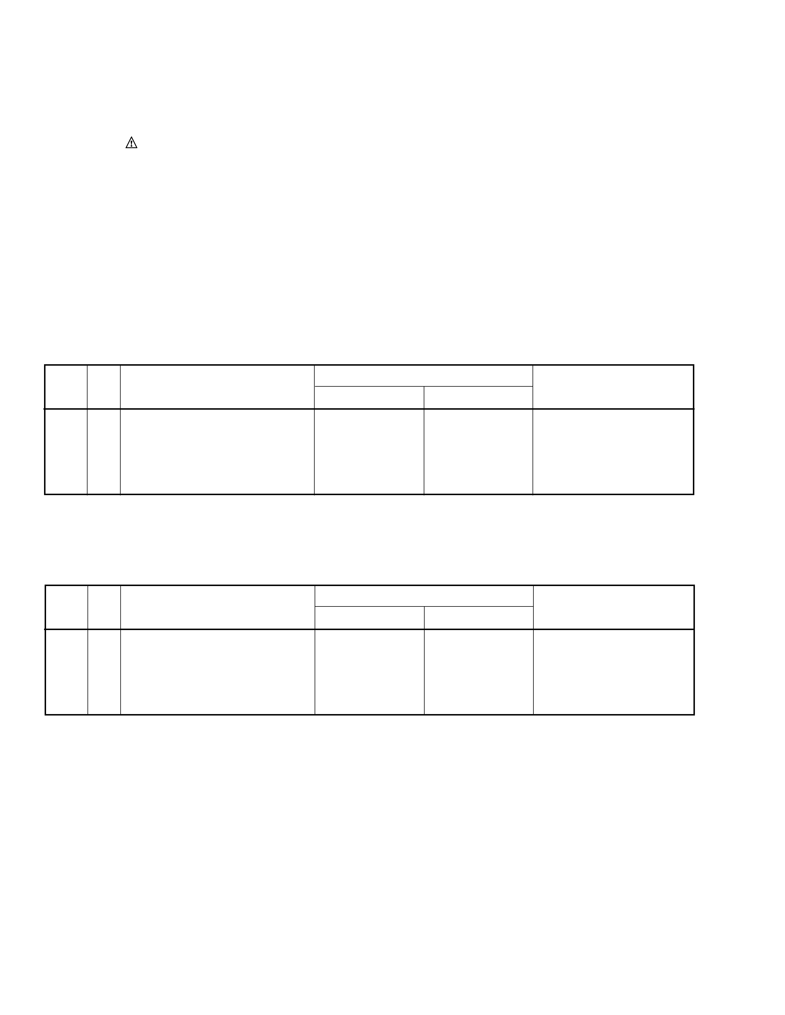
7 CONTRAST TABLE FOR KU/CA2 TYPE
KU/CA2 type and KU/CA type are constructed the same except for the following:
ASSEMBLIES
P7 8
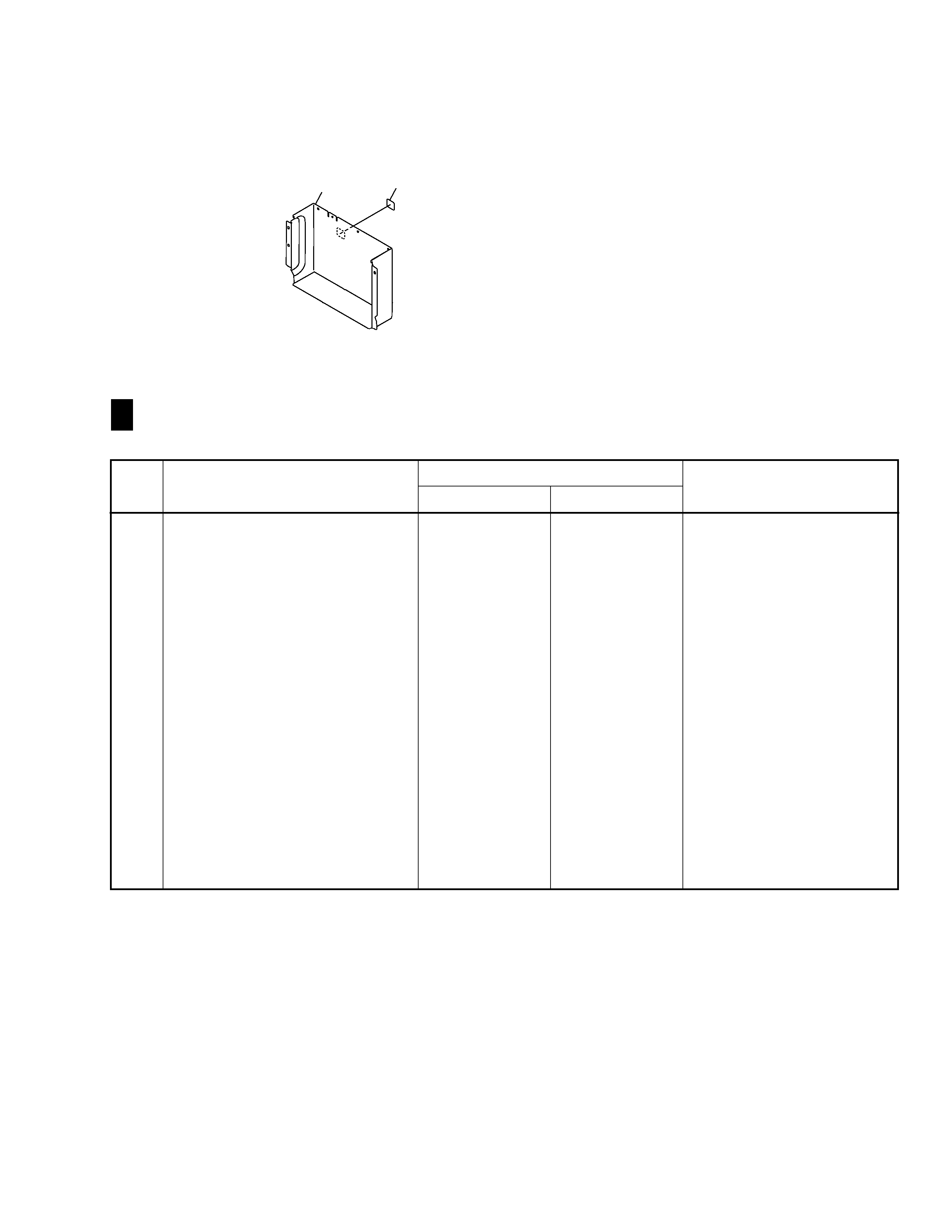
DVDM ASSY
VWS1377
VWS1397
BOTTOM VIEW SECTION
P929
REAR COVER
VNA2028
VNA2144
Ref.
No.
Remarks
KU/CA type
KU/CA2 type
Part No.
Mark
Symbol and Description
NOTES :
÷ Parts marked by " NSP " are generally unavailable because they are not in our Master Spare Parts List.
÷ The
mark found on some component parts indicates the importance of the safety factor of the part.
Therefore, when replacing, be sure to use parts of identical designation.
÷ Reference Nos. indicate the pages and Nos. in the service manual for the base model.
÷ When ordering resistors, first convert resistance values into code form as shown in the following examples.
Ex. 1
When there are 2 effective digits (any digit apart from 0), such as 560 ohm and 47k ohm (tolerance is shown by
J = 5%, and K = 10%).
560
= 56 × 101= 561 ................................................... RD1/4PU 5 6 1 J
47k
= 47 × 10 3 = 473 .................................................. RD1/4PU 4 7 3 J
0.5
= R50 ...................................................................... RN2H Â 5 0 K
1
= 1R0 ......................................................................... RS1P 1 Â 0 K
Ex. 2
When there are 3 effective digits (such as in high precision metal film resistors).
5.62k
= 562 × 10 1 = 5621 ........................................... RN1/4PC 5 6 2 1 F
¶ For PCB ASSEMBLIES, Refer to "CONTRAST OF PCB ASSEMBLIES", "2. SCHEMATIC DIAGRAM" and "3. PCB CONNECTION DIAGRAM".
7 CONTRAST TABLE FOR RD/RA2 TYPE
RD/RA2 type and RD/RA type are constructed the same except for the following:
ASSEMBLIES
P7 8
DVDM ASSY
VWS1377
VWS1397
BOTTOM VIEW SECTION
LABEL
Not used
VRW1789
No. 1
Ref.
No.
Remarks
RD/RA type
RD/RA2 type
Part No.
Mark
Symbol and Description
¶ The numbers in the remarks column correspond to the numbers on the "EXPLODED VIEWS".
¶ For PCB ASSEMBLIES, Refer to "CONTRAST OF PCB ASSEMBLIES", "2. SCHEMATIC DIAGRAM" and "3. PCB CONNECTION DIAGRAM".
 I Service Manual")