4
CX-683
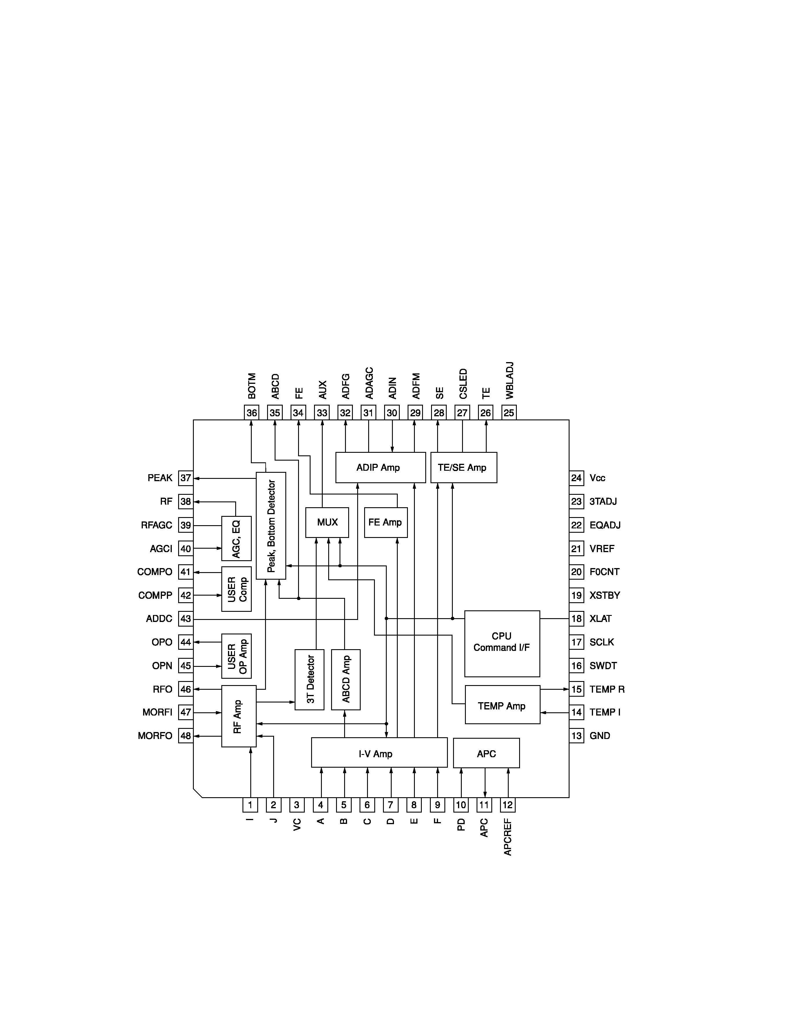
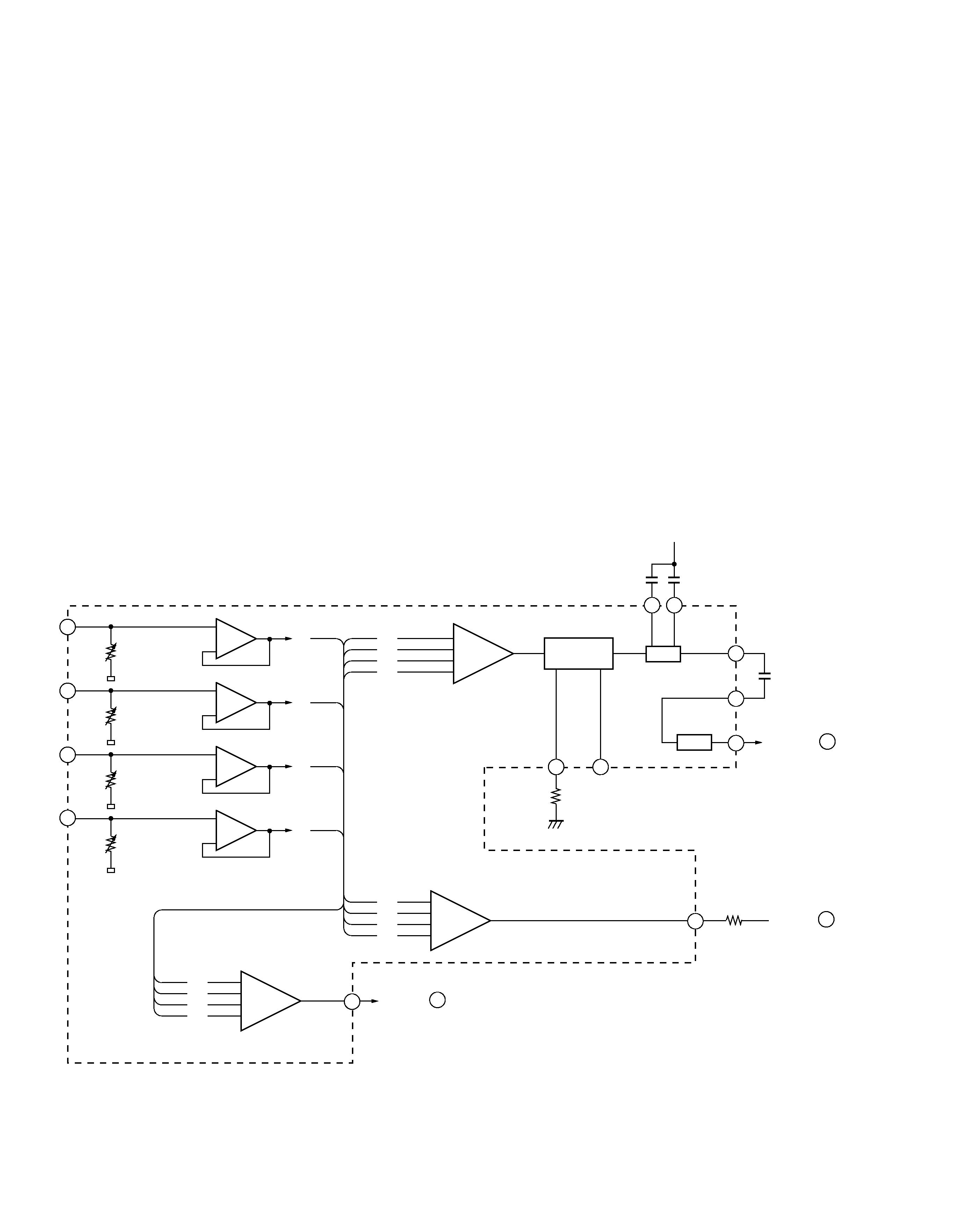
3) I-V, ADIP, ABCD and FE Amplifier Blocks
They are used for I-V conversion of photo-detector signals (A to F pins) from the pickup.
ADIP, FE and full quantity of light signals are generated from A to D signals, and TE signal is generated from E and F
signals.
The ABCD amplifier generates the full quantity of light signal for the main spot. This signal is sum of A to D signals
after I-V conversion. According to the level of the full quantity of light signal, resistance value of I-V is automatically
adjusted so that ADIP, FE and TE signals may be maintained at the specified level.
FE and TE signals output from both the Recordable and Premastered Discs are adjusted to approximately 1 Vpp and
1.7 Vpp, respectively. This adjustment is executed whenever a disc is inserted.
ABCD signal entered to the signal processing LSI (IC201: 64 pins) is also used for generating FOK and defect detect
signals.
The ADIP amplifier is used for generating ADIP signal that is present only on the Recordable Disc.
Addresses are already recorded on the Recordable Disc by wobbling FM signal that uses 22.05 KHz as the carrier. In
order to detect wobble elements, noise elements of the signal are eliminated on the BPF, then the signal is output to
the ADFM via the AGC. The signal is then sent to C111 for DC cut and binary converted on the comparator to generate
ADFG signal. ADFG signal is entered to the signal processing LSI (IC201: 78 pins) to control the address and spindle
when the Recordable Disc is played.
+
+
4
+
5
+
6
+
7
25
+
+
+
35
64
34
29
30
32
65
78
20
43
31
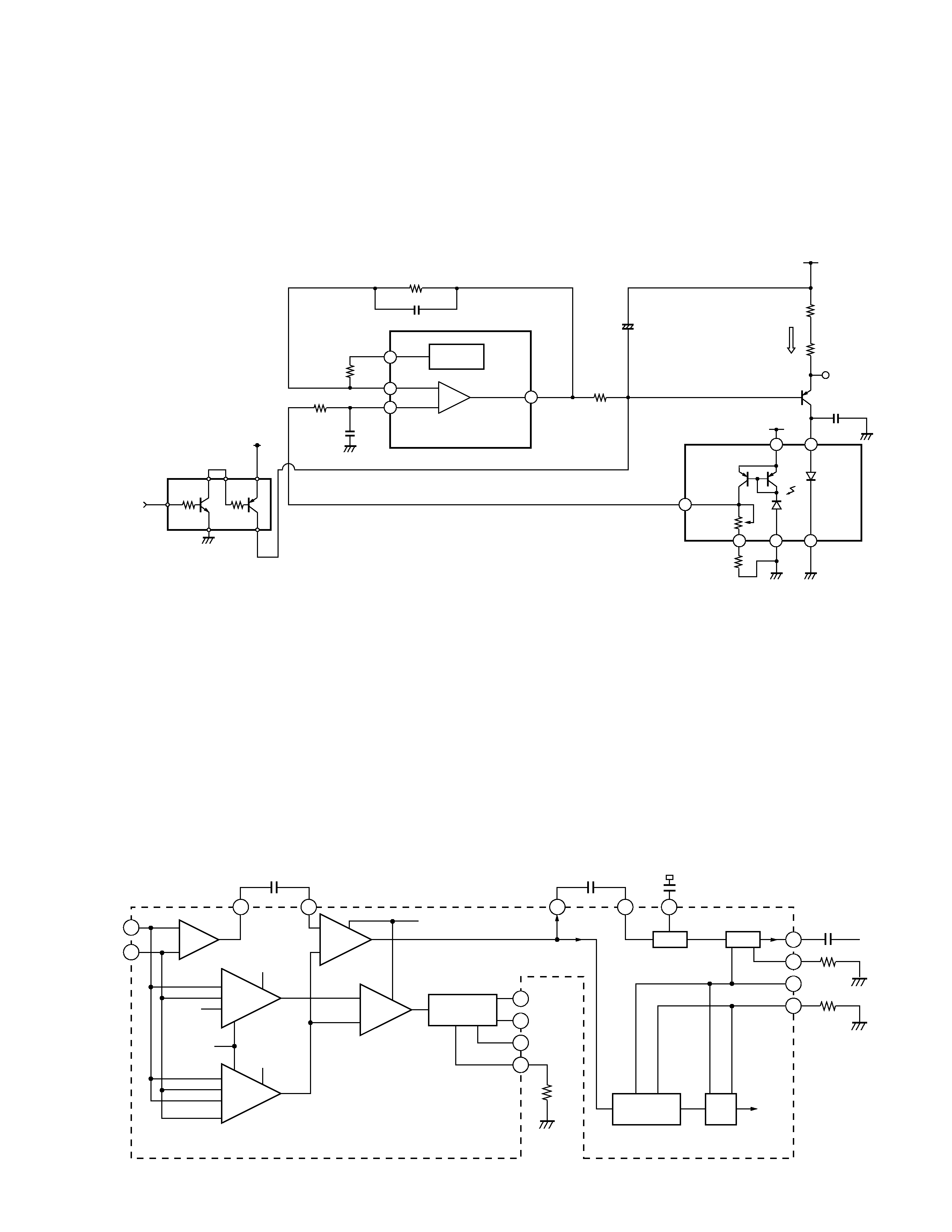
Focus err amplifier
IVR0-IVR4
FE R219
100
AIV
A
AA
BB
CC
AA
DD
AA
CC
BB
DD
AA
BB
CC
DD
IVR0-IVR4
BIV
B
ABCD
BB
IVR0-IVR4
CIV
C
CC
IVR0-IVR4
DIV
ABCDA
FEA
ATA
D
DD
ADAGC
ADFM
ADIN
WBLADI
F0CNT
ADFG
ADDC
C11
4700P
<To IC201
pins>
BPF
fo=22.05kHz
BPF22
ADIPAGC
<To IC201
pins>
<To IC201
pins>
AGC
BPFC
COMP
ABCD amplifier
I-V amplifier
ADIP amplifier