PIONEER CX-3026 Service Manual

Cover page of PIONEER CX-3026 Service Manual

Service Manual for PIONEER CX-3026, downloadable as a PDF file.

Manual details

  • Immediate download after payment.
  • Delivered as a PDF file.
  • The manual has 25 pages
  • File size: 4.93 MB
  • Available language versions: English
  • Different language versions may vary sligthly in file size and page count.

We guarantee that...

  • our manuals are complete,
  • the manual includes circuit diagrams,
  • our manuals are checked with antivirus,
  • We'll issue refund if the manual is damaged, incomplete or unreadable (our refund policy)

Sample pages

Thumbnail of page 1Thumbnail of page 2Thumbnail of page 3Thumbnail of page 4
Thumbnail of page 5Thumbnail of page 6Thumbnail of page 7Thumbnail of page 8
Thumbnail of page 9
background image
PIONEER CORPORATION
4-1, Meguro 1-Chome, Meguro-ku, Tokyo 153-8654, Japan
PIONEER ELECTRONICS (USA) INC.
P.O.Box 1760, Long Beach, CA 90801-1760 U.S.A.
PIONEER EUROPE NV
Haven 1087 Keetberglaan 1, 9120 Melsele, Belgium
PIONEER ELECTRONICS ASIACENTRE PTE.LTD. 253 Alexandra Road, #04-01, Singapore 159936
C PIONEER CORPORATION 2002
K-ZZA. NOV. 2002 Printed in Japan
ORDER NO.
CRT2944
CD MECHANISM MODULE
CX-3026
Service
Manual
Model
Service Manual
CD Mechanism Module
DEH-P250/XM/UC
CRT2981
CXK5600
DEH-P250/XN/UC
DEH-P2500/XM/UC
DEH-P2500/XN/UC
DEH-P25/XM/UC
DEH-P25/XN/UC
DEH-P2530R/XM/EW
CRT2982
DEH-P2530R/XN/EW
DEH-P2500R/XM/EW
DEH-P2500R/XN/EW
DEH-P2500RB/XM/EW
DEH-P2500RB/XN/EW
DEH-P2550/XM/ES
CRT2983
DEH-P2550/XN/ES
DEH-P350/XM/UC
CRT2984
DEH-P350/XN/UC
DEH-P3500/XM/UC
DEH-P3500/XN/UC
DEH-P4550/XM/ES
DEH-P4550/XN/ES
DEH-P4500R/XM/EW
CRT2985
DEH-P4500R/XN/EW
- This service manual describes the operation of the CD mechanism module incorporated in models list-
ed in the table below.
- When performing repairs use this manual together with the specific manual for model under repair.
CONTENTS
1. CIRCUIT DESCRIPTIONS ...........................................2
2. MECHANISM DESCRIPTIONS.................................20
3. DISASSEMBLY .........................................................22
background image
2
1
234
12
34
F
E
D
C
B
A
CX-3026/E
1. CIRCUIT DESCRIPTIONS
Recently, Many CD LSIs have been one-chip LSIs where RF amplifier, DSP, audio DAC, post filter, and other circuits are
integrated.
This product uses this type CD LSI, UPD63712GC, which includes all functions necessary for CD player control.
Basically, this system outputs the analog signal, and the digital output can be supported.
Fig.1.0.1 Block diagram of CD LSI UPD63712GC
Servo
PWM output
CD-TEXT
A-F
EFM
Digital signal
processing
A/D converter
RF amplifier
UPD63712GC
1 bit,
Audio DAC
Post filter
(SCF)
Analog output
Microcomputer
for system control
MPU interface
Digital servo
Drive output
background image
3
5
6
7
8
F
E
D
C
B
A
5
6
7
8
CX-3026/E
1.1 PREAMPLIFIER BLOCK (UPD63712GC: IC201)
In the preamplifier block, the pickup output signals are processed to generate signals that are used for the next-stage
blocks: the servo block, demodulator, and control.
After I/V-converted by the preamplifier with built-in photo detectors (inside the pickup), the signals are applied to the
preamplifier block in the CD LSI UPD63712GC (IC201). After added by the RF amplifier in this block, these signals are
used to produce necessary signals such as RF, FE, TE, and TE zero-cross signals.
The CD LSI employs a single power supply system of + 3.3V. Therefore, the REFO (1.65V) is used as the reference volt-
age both for this CD LSI and the pickup. The LSI produces the REFO signal by using the REFOUT via the buffer amplifi-
er and outputs from the pin 90. All the measurements should be made based on this REFO.
Caution: Be careful not to short the REFO and GRD when measuring.
1.1.1 APC (Automatic Power Control)
A laser diode has extremely negative temperature characteristics in optical output at constant-current drive. To keep
the output constant, the LD current is controlled by monitor diodes. This is called the APC circuit. The LD current is
calculated at about 30mA, which is the voltage between LD1 and V+3A divided by 7.5 (ohms).
Fig. 1.1.1 APC
6.5 k
+
-
1 k
100 k
+
-
150 k
100 k
+
-
110 k
1 k
REG 1.25V
Vref
3 p
1
3
PD
PN
LD
UPD63712GC
2
+
100
p
R1
R1
5
7
15
5
7
15
14
14
Pickup Unit(P10)
CD CORE UNIT(S10)
1R5
x
5
2SB1132
1SS355
100/16
LD-
LD+
MD
VR
LDS
APN
3 p
APC REG 1.25V
background image
4
1
234
12
34
F
E
D
C
B
A
CX-3026/E
1.1.2 RF and RFAGC amplifiers
The photo-detector outputs (A + C) and (B + D) are added, amplified, and equalized inside this LSI, and then provided
as the RF signal from the RFI terminal. The RF signal can be used for eye-pattern check.
The low frequency component of the RFI voltage is:
RFO = (A + B + C + D) x 2
The RFO is used for the FOK generation circuit and RF offset adjustment circuit.
The RFI output from the pin 71 is A/C-coupled outside this LSI, and returned to the pin 76 of this LSI. The signal is
amplified in the RFAGC amplifier to obtain the RFAGC signal. This LSI is equipped with the RFAGC auto-adjustment
function as explained below. This function automatically controls the RFO level to keep at 1.5V by switching the feed-
back gain for the RFAGC amplifier.
The RFO signal is also used for the EFM, DFCT, MIRR, and RFAGC auto-adjustment circuits.
Fig. 1.1.2 RF/AGC/FE
13
6
A+C
B+C
VREF
13
6
10 k
10 k
8.8 k
10 k
10 k
8.8 k
61 k
61 k
140 k
R2
15.2 k
15.2 k
44 k
20 k
11.75 k
3.55 k
5 k
5 k
82
85
83
84
75
72
73
76
93
92
VREF
VREF
A
B
C
D
RFO
AGCI
RF2-
RF-
EQ2
EQ1
AGCO
FEO
FE-
FE A/D
77
78
+
-
+
-
+
-
+
-
+
-
+
-
-
+
P3
P7
P9
P2
P4
P8
Pickup Unit(P10)
CD CORE UNIT(S10)
UPD63712GC
1.2 k
20 p
74
R1
1.2 k
47 p
3 p
2 p
RFOFF setup
FEOFF setup
For RFOK generation
To DEFECT/A3T detection
background image
5
5
6
7
8
F
E
D
C
B
A
5
6
7
8
CX-3026/E
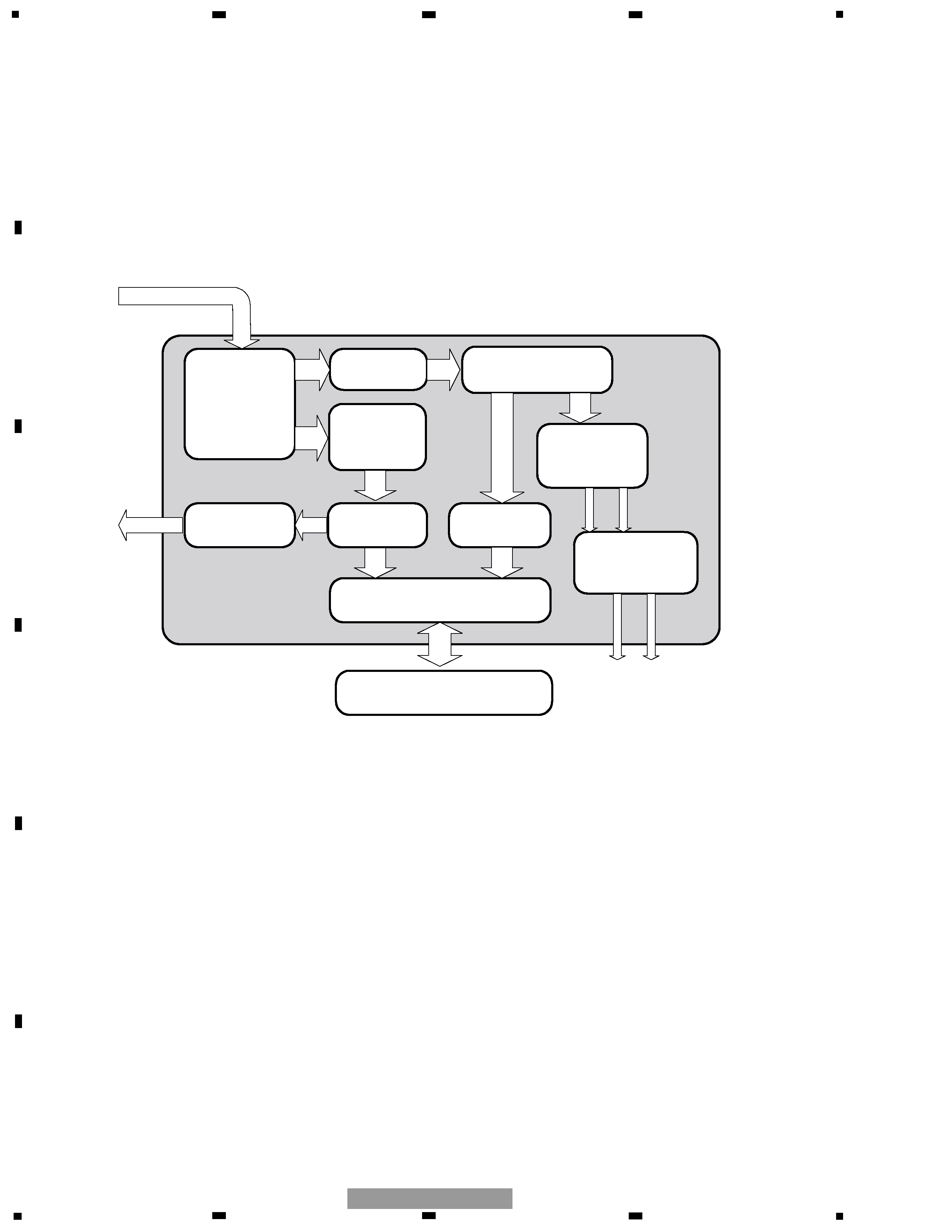
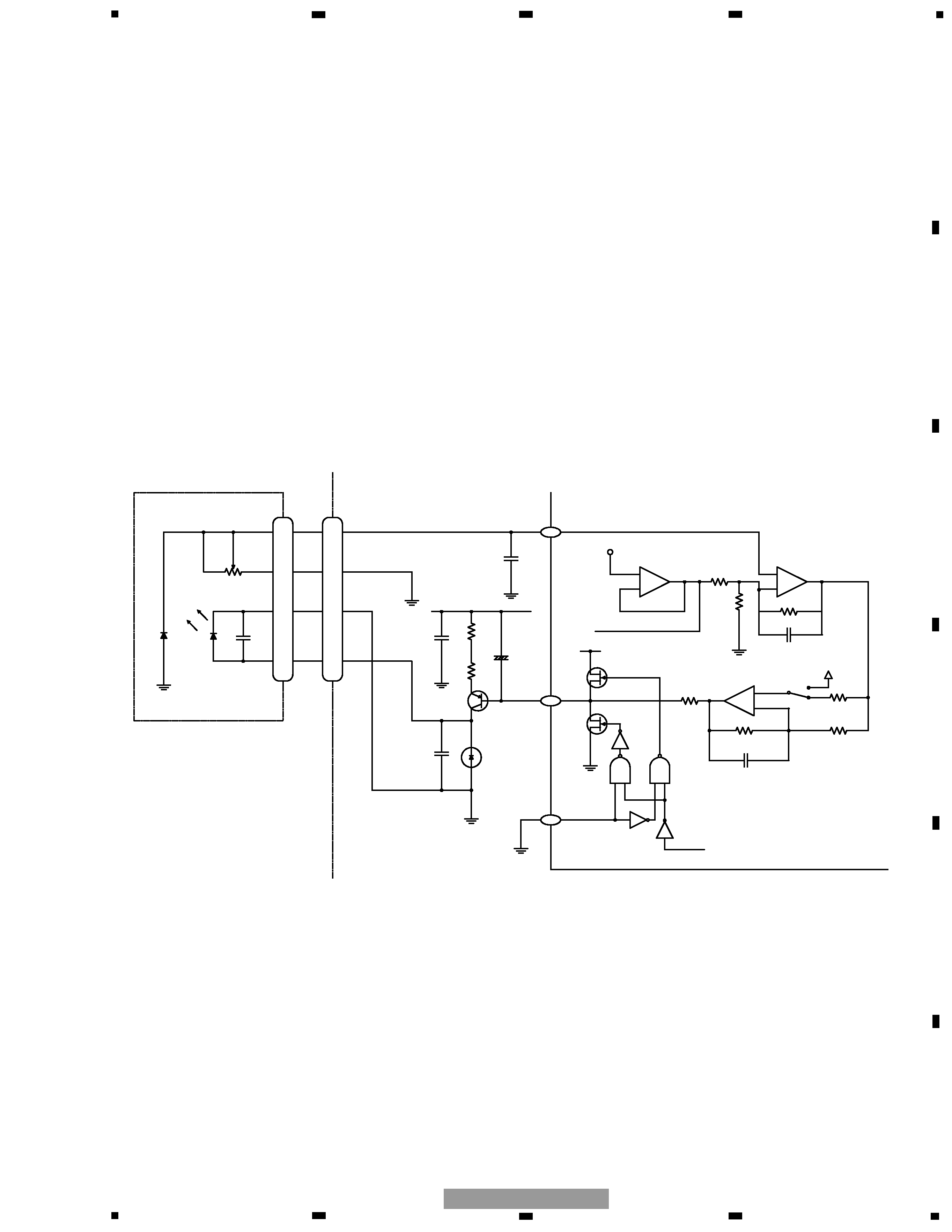
1.1.3 Focus error amplifier
The photo-detector outputs (A + C) and (B + D) are applied to the differential amplifier and the error amplifier to obtain
the (A + C - B - D) signal, which is then provided from the pin 93 as the FE signal.
The low frequency component of the FE voltage is:
FE = (A + C - B - D) x 8.8k/10k x 111k/61k x 160k/72k
= (A + C - B - D) x 3.55
The FE output shows 1.5Vp-p S-shaped curve based on the REFO. For the next-stage amplifiers, the cutoff frequency
is 14.6kHz.
1.1.4 RFOK
The RFOK circuit generates the RFOK signal, which indicates focus-close timing and focus-close status during the play
mode, and outputs from the pin 6. This signal is shifted to "H" when the focus is closed and during the play mode.
The DC level of the RFI signal is peak-held in the digital block and compared with a certain threshold level to generate
the RFOK signal. Therefore, even on a non-pit area or a mirror-surface area of a disc, the RFOK becomes "H" and the
focus is closed.
This RFOK signal is also applied to the microcomputer via the low-pass filer as the FOK signal, which is used for pro-
tection and RF amplifier gain switching.
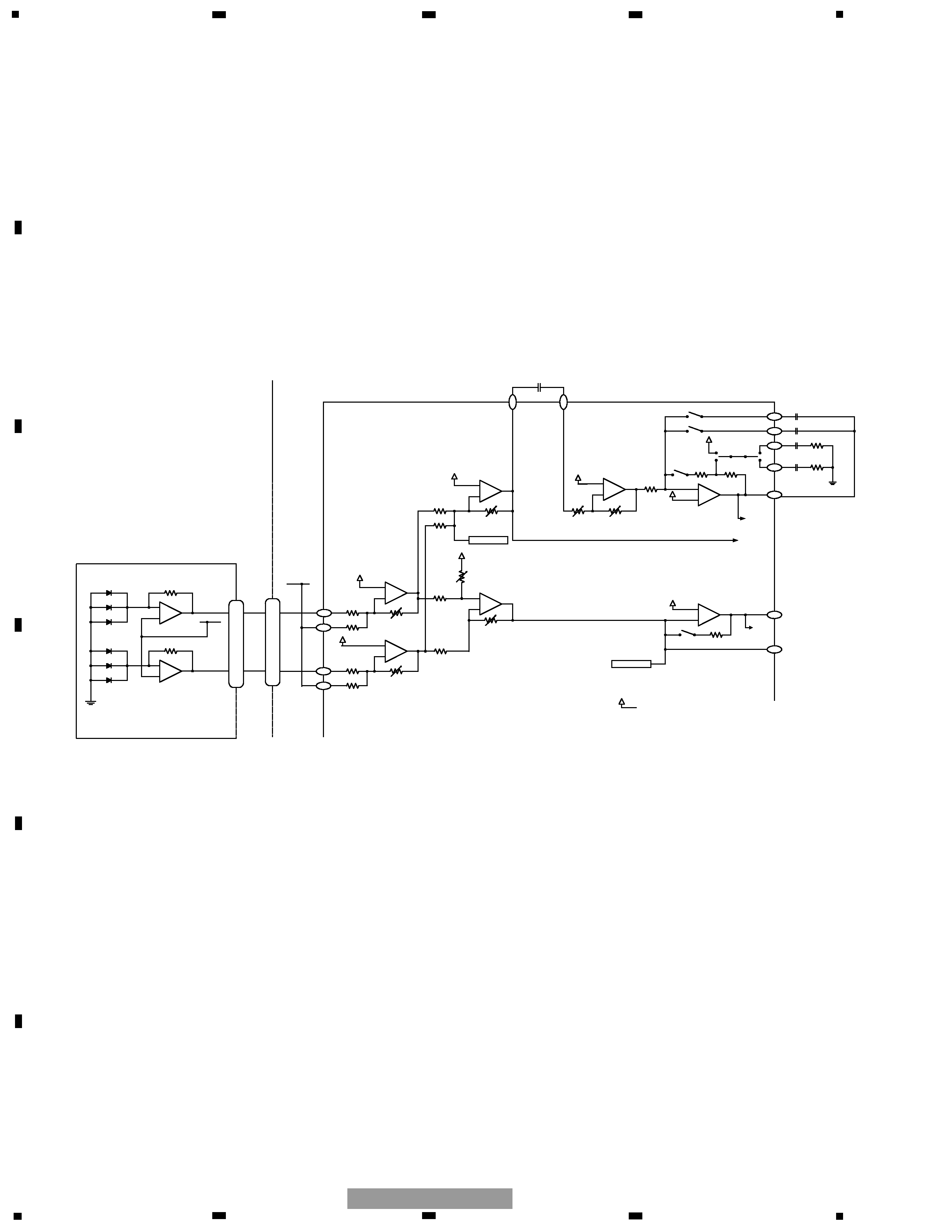
1.1.5 Tracking error amplifier
The photo-detector outputs E and F are applied to the differential amplifier and the error amplifier to obtain the (E - F)
signal, and then provided from the pin 96 as the TE signal.
The low frequency component of the TE voltage is:
TEO = (E - F) x 63k/112k x 160k/160k x 181k/45.4k x 160k/80k
= (E - F) x 4.48
The TE output provides the TE waveform of about 1.16Vp-p based on the REFO. For the next-stage amplifiers, the cut-
off frequency is 21.1kHz.
Fig. 1.1.3 TE
11
9
E
F
VREF
11
9
112 k
112 k
63 k
45.4 k
63 k
160 k
160 k
45.4 k
161 k
80 k
160 k
60 k
20 k
87
86
TE A/D
Pickup Unit(P10)
P5
P10
P1
P6
E
F
UPD63712GC
CD CORE UNIT(S10)
+
-
+
-
+
-
+
-
+
-
+
-
-
+
VREF
TEO
TE-
TEC
TE2
96
95
97
98
33 p
R1
Inside TEC
TEOFF setup

Reviews

There are no reviews of this manual yet.