PIONEER AVH-P5900DVD/XN/UC Service Manual

Cover page of PIONEER AVH-P5900DVD/XN/UC Service Manual

Service Manual for PIONEER AVH-P5900DVD/XN/UC, downloadable as a PDF file.

We also have owner's manual to this model.

Manual details

  • Immediate download after payment.
  • Delivered as a PDF file.
  • The manual has 32 pages
  • File size: 1.89 MB
  • Available language versions: English
  • Different language versions may vary sligthly in file size and page count.

We guarantee that...

  • our manuals are complete,
  • the manual includes circuit diagrams,
  • our manuals are checked with antivirus,
  • We'll issue refund if the manual is damaged, incomplete or unreadable (our refund policy)

Sample pages

Thumbnail of page 1Thumbnail of page 2Thumbnail of page 3Thumbnail of page 4
Thumbnail of page 5Thumbnail of page 6Thumbnail of page 7Thumbnail of page 8
Thumbnail of page 9
background image
ORDER NO.
PIONEER CORPORATION 4-1, Meguro 1-chome, Meguro-ku, Tokyo 153-8654, Japan
PIONEER ELECTRONICS (USA) INC. P.O. Box 1760, Long Beach, CA 90801-1760, U.S.A.
PIONEER EUROPE NV Haven 1087, Keetberglaan 1, 9120 Melsele, Belgium
PIONEER ELECTRONICS ASIACENTRE PTE. LTD. 253 Alexandra Road, #04-01, Singapore 159936
PIONEER CORPORATION 2007
CRT3896
DVD MECHANISM MODULE(MS5)
CX-3212
K-ZZU. FEB. 2007 Printed in Japan
CONTENTS
1. CIRCUIT DESCRIPTIONS................................................................................................................................ 2
2. MECHANISM DESCRIPTIONS ...................................................................................................................... 19
3. DISASSEMBLY ............................................................................................................................................... 24
- This service manual describes the operation of the DVD mechanism module incorporated in models
listed in the table below.
- When performing repairs use this manual together with the specific manual for model under repair.
Model
Service manual
DVD Mechanism Module
AVIC-D3/XU/UC
CRT3879
CXK6601
AVIC-D3/XU/EW5
background image
CX-3212
2
12
3
4
12
3
4
C
D
F
A
B
E
1. CIRCUIT DESCRIPTIONS
1. Front end section (MN2DS0016AAUB : IC1501)
MN2DS0016AAUB is a 1 chip LSI for DVD-Player. A DVD-Player system can be constructed by connecting this LSI,
driver IC, SDRAM, Flash-ROM, Audio-DAC, etc.
This LSI includes a front end (SODC/FE) which executes RF signal processing, servo processing and decode
processing, a back end (AV decoder/BE) which executes video decode processing such as MPEG1/MPEG2/JPEG
and audio decode processing such as DVD-Audio/Dolby Digital /DTS/MP3, and a system controller which controls
the system.
The front end section realizes optical head signal computation processing and RF signal processing, digital signal
processing (16-8 demodulation, error correction) for DVD-ROM playback according to the DVD specifications,
digital signal processing of CD-DA/CD-ROM (error correction), AV decoder transfer, servo control, spindle motor control
and seek control.
In the case of MN2DS0016AAUB, the front end servo system waveforms, such as FE, TE and AS, are not observed
as in the case of DVD mechanism module (MS4) CX-3183. Please pay attention.
1.1 Analog block (MN2DS0016AAUB : IC1501)
The functions of the analog block are as described below.
1. Reference power circuit
2. SERVO system/DPD system signal processing circuit
Gain switching amplifier and Low Pass Filter (LPF)
3. RF signal processing circuit
RF adding circuit, circuit to make inline, Variable Gain Amplifier (VGA) circuit
4. Laser power control (LPC) circuit
5. A/D converter for SERVO (10 bit, DPD system-4ch), PWM
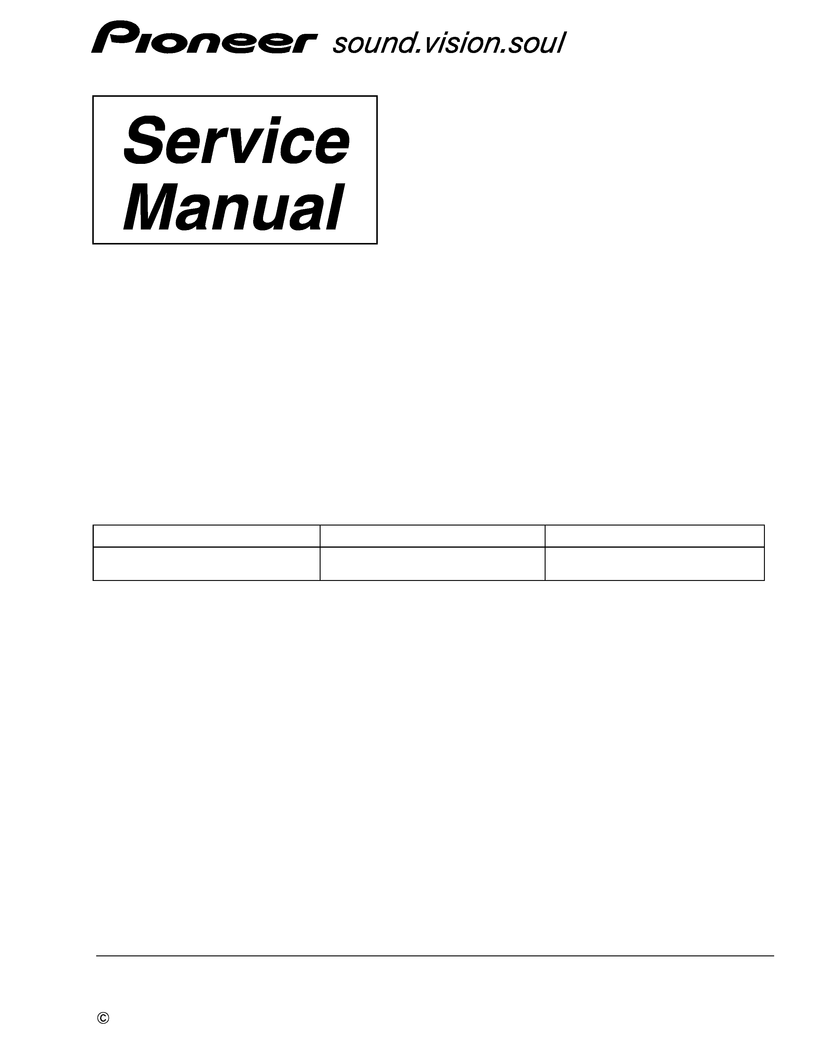
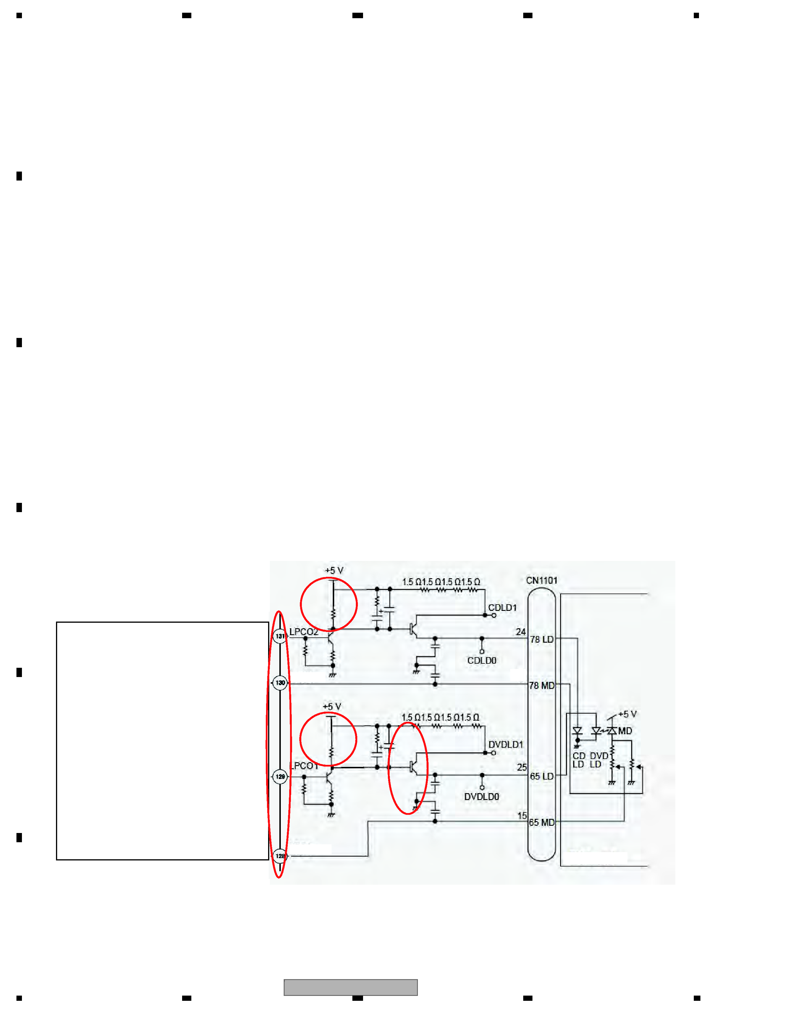
1.1.1 APC circuit
The optical output of the laser diode (LD) has a large negative temperature characteristic.
Therefore, if the LD is driven by a constant current, a constant optical output cannot be obtained.
APC circuit is a circuit to control the current so that the output at the monitor diode (MD) will be constant.
MN2DS0016AAUB includes 2 types of APC circuit, one for DVD and the other for CD.
The LD current can be obtained by dividing the measured voltage between DVDLD1 (CDLD1) and 5 V by 6
(1.5
x 4=6 ), in the case of DVD (CD). It will be approximately 50 mA (45 mA) in the case of DVD (CD).
The potential difference between DVDLD1(CDLD1) and 5 V is set to approx. 300 mV(270 mV).
DVN Chip
(MN2DS0016AAUB : IC1501)
CDMPD
14
DVDMPD
PU UNIT
2
background image
CX-3212
3
5
678
56
7
8
C
D
F
A
B
E
1.1.2
FE
forming
circuit
Focus
error
(FE)
forming
circuit
The
signal
from
PU,
FE1
and
FE2,
are
AD
converted
inside
IC1501
and
captured.
After
that,
a
differential
is
obtained
by
taking
the
offset
cancellation
into
consideration,
and
FE
is
obtained.
FE
=
(FE1)
-
(FE2)
12
11
FE2
FE1
CN1101
136
137
VIN5
VIN6
Input
AMP
Gain
switching
-6
dB,
0
dB,
9.5
dB
LPF
50
k/100
kHz
LPF
Buffer
LPF
50
k/100
kHz
G=0
dB
Buffer
AMP
Selector
Selector
Gain
switching
3
dB,
9
dB
DVN
Chip
ADC
driving
AMP
Gain
switching
6/7.5/9/10.5/
12/13.5/15/
16.5/17/19.5
dB
ADC
ADC
After
10
bit
ADC
FE
signal
forming
circuit
1+Pfbal0,1/0x0100
1-Pfbal0,1/0x0100
Offset
cancel
Fbal
coarse
adjustment
value
FE
AMP
DVN
Chip
FE1
FE2
+
-
background image
CX-3212
4
12
3
4
12
3
4
C
D
F
A
B
E
1.1.3
TE
forming
circuit
Tracking
error
(TE)
forming
circuit
In
the
case
of
a
DVD,
the
phase
difference
method
is
used
for
TE
forming,
and
the
TE
is
formed
from
the
phase
difference
among
(A+C)
and
(B+D).
In
the
case
of
a
CD,
3
beam
method
is
used,
and
after
entering
the
signal
into
a
variable
amplifier
for
tracking
offset
adjustm
ent
via
an
external
resistor,
it
is
AD
converted,
and
a
TE
is
formed
by
the
equation
of
TE=(E+G_E+F)-(F+H_G+H).
DVD
(phase
difference
TE)
A
B
C
D
CN1101
0.1
F
0.1
F
0.1
F
0.1
F
7
8
9
10
121
123
VIN3RF
VIN1RF
120
VIN4RF
122
VIN2RF
Gain
switching
­7.5
dB,
0
dB,
3.5
dB
LPF
27
M/11.3
M
/5.7
MHz
Input
AMP
LPF
LPF
27
M/11.3
M
/5.7
MHz
LPF
27
M/11.3
M
/5.7
MHz
LPF
27
M/11.3
M
/5.7
MHz
Buffer
Gain
switching
G=0,3,6,9,12,15
dB
HPF
HPF
100
kHz
HPF
100
kHz
HPF
100
kHz
HPF
100
kHz
G=-1
dB
ADC1
ADC4
ADC
ADC2
ADC3
AMP
DVN
Chip
Phase
comparator
Phase
comparator
LPF
(integrator)
D
+
TE
signal
forming
circuit
AMP
TE
+
background image
CX-3212
5
5
678
56
7
8
C
D
F
A
B
E
CD
(3
beam
TE)
CN1101
F+H_
G
+
H
E+
G_E+
F
21
22
134
135
VIN10
VI
N9
Gain
switching
-6
dB,
0
dB,
9.5
dB
Input
AMP
LPF
50
k/100
kHz
LPF
G=0
dB
Buffer
LPF
50
k/100
kHz
Buffer
AMP
Gain
switching
3
dB,
9
dB
Gain
switching
6/7.5/9/10.5/
12/13.5/15/
16.5/17/19.5
dB
ADC
Selector
Selector
ADC
AMP
DVN
Chip
After
10
bit
ADC
E+
G
_E+
F
F+
H
_G
+
H
TE
signal
forming
circuit
+
-
1+Ptbal0,1/0x0100
1-Ptbal0,1/0x0100
Offset
cancel
Tbal
adjustment
value
DVN
Chip
TE
AMP

Reviews

There are no reviews of this manual yet.