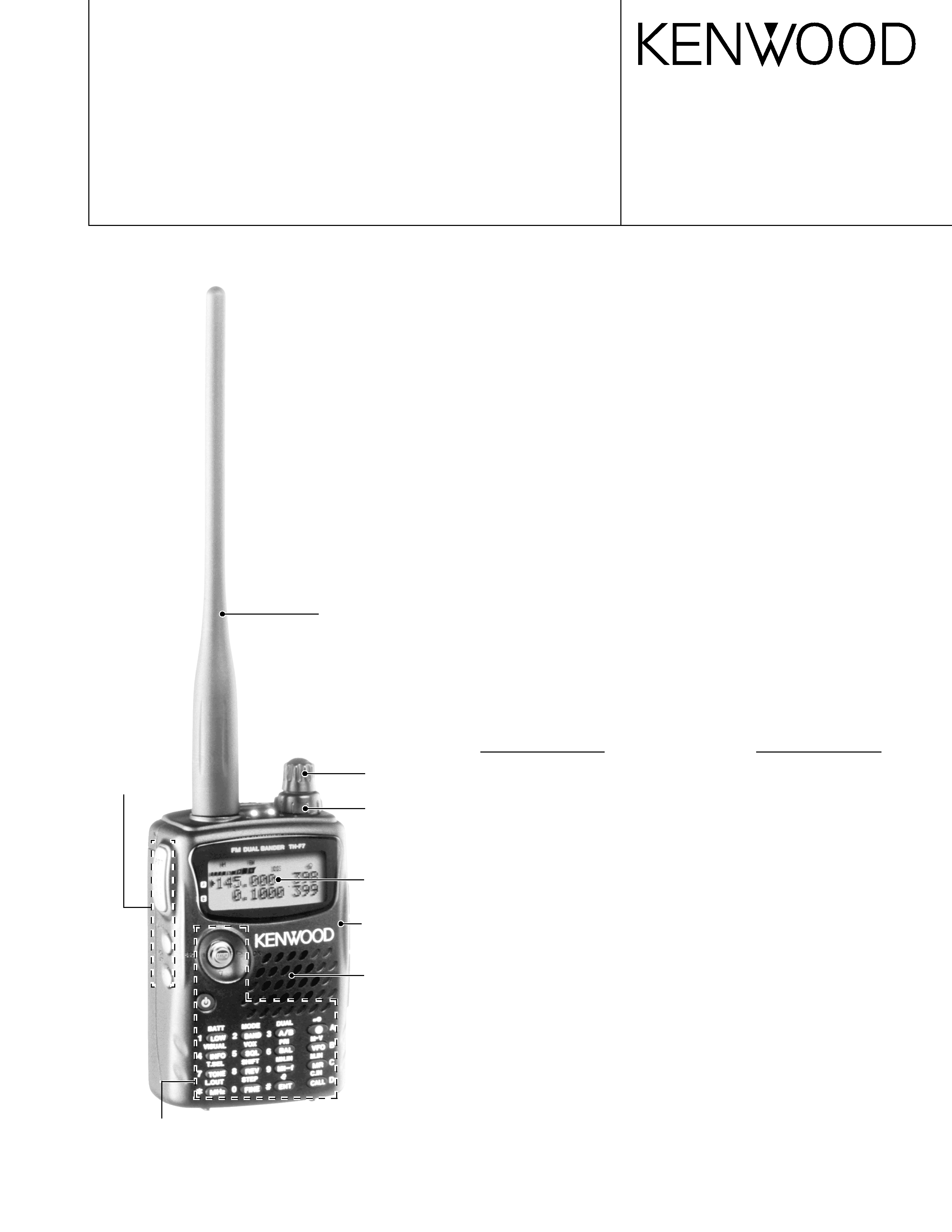
TH-F6A/F7E
5
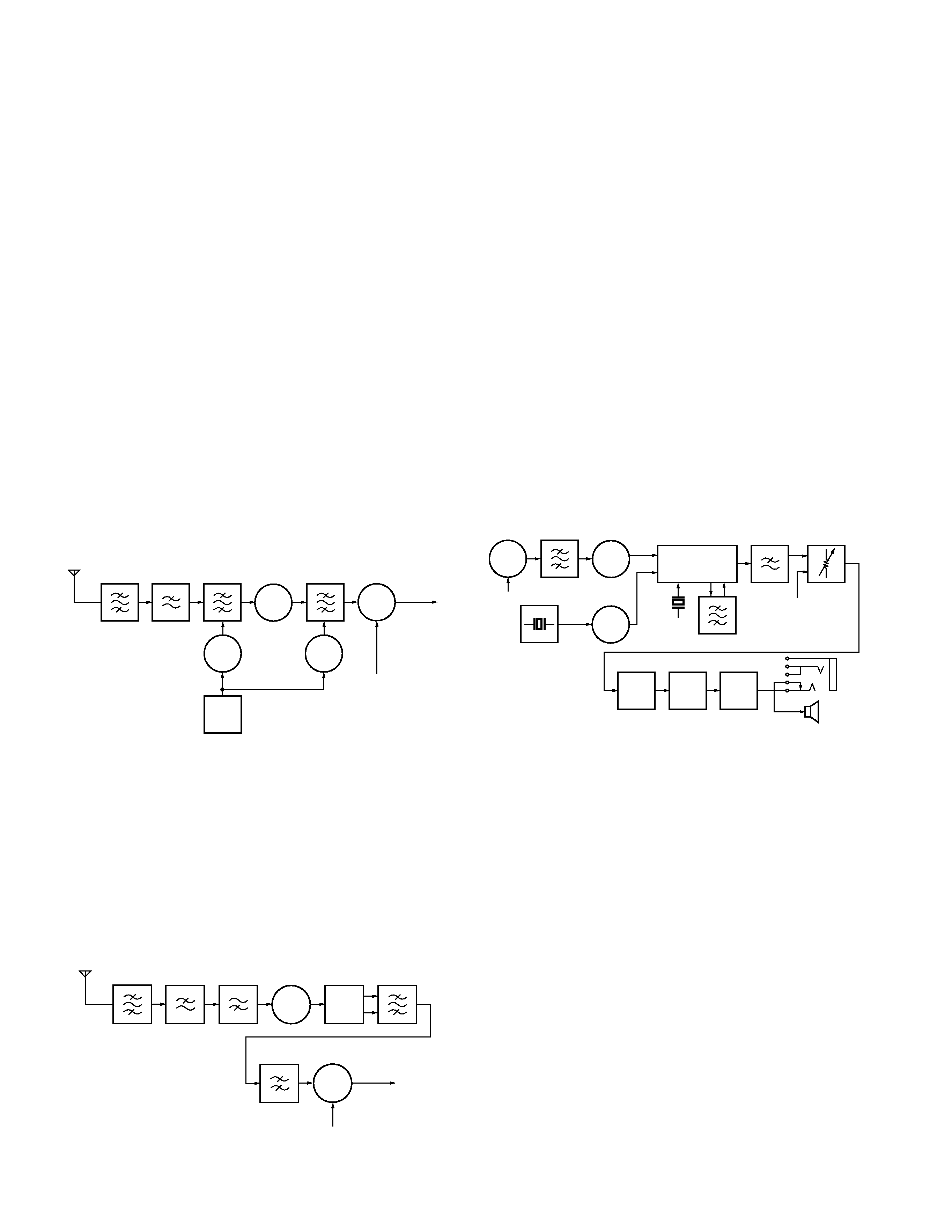
CIRCUIT DESCRIPTION
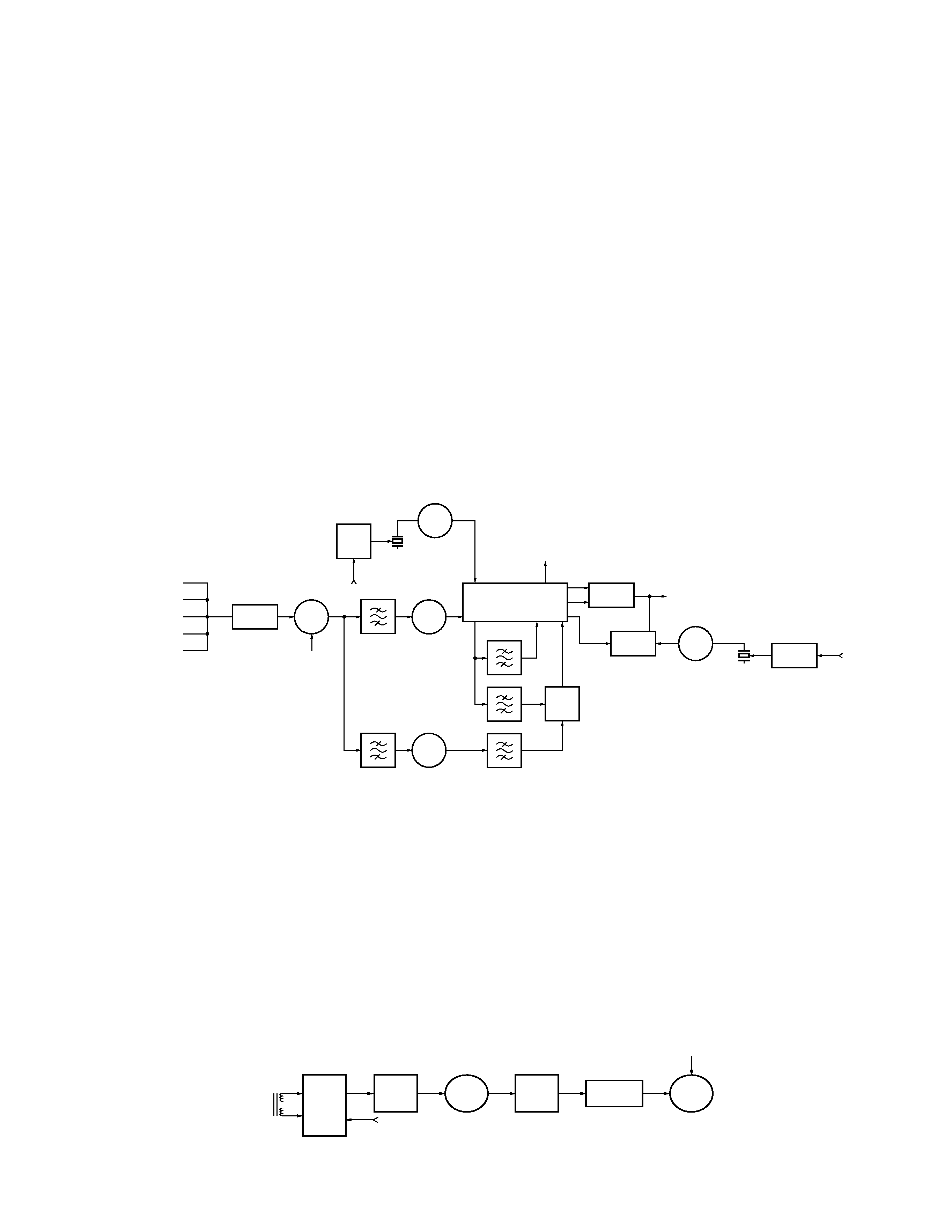
Fig.4
The first amplifier is divided into four bands: 100 kHz - 50
MHz, 50MHz - 108MHz, 108 MHz - 265 MHz, 265 MHz - 600
MHz, and 600 MHz - 1.3 GHz. The incoming signal from the
antenna passes through a low-pass filter and a duplexer, and
goes to an independent amplifier for each band. Then, the
signal goes to the second common broadband amplifier (IC10)
and its output is fed to the mixer (Q28) and heterodowned to
the first IF.
2-1-1. FM/AM receiver circuit
The signal heterodowned to the first IF of 57.6MHz passes
through a 15kHz MCF (XF1), and unwanted signal components
are eliminated. The resulting signal is amplified by the IF
amplifier (Q26) and goes to the FM IC (IC5). The FM IC
heterodowns it to the second IF of 450 kHz. In FM mode, the
signal passes through a 12.0kHz external ceramic filter (CF3)
and goes to the FM IC. The signal amplified by the internal IF
amplifier is demodulated by the quadrature FM demodulation
circuit using a coil (L19) and converted into an audio signal
and output. In AM mode, the signal passes through a 4kHz
external ceramic filter CF1 and goes back to the FM IC. It is
amplified by the AM AGC amplifier built in the FM IC, an audio
output from the FM IC as an audio signal.
2-1-4. AM bar antenna receiver circuit
This unit incorporates an AM bar antenna, and either the
bar antenna or the supplied antenna can be selected in the
520kHz-1.8MHz (SW) and 3.5MHz-10.1MHz (MW) bands (the
initial value: bar antenna). The bar antenna has two kinds of
tuners for SW and MW tuning, one of which is selected with a
switching FET (Q32, Q48, Q52). The antenna is tuned with a
varicap (D60) for AM tuning to select a desired signal. The
signal from the bar antenna is amplified by and its impedance
is converted by the buffer amplifier (Q59), and the resulting
signal goes to the common mixer (Q28) for the B band. The
signal is routed over the same path for AM demodulation as
for the supplied antenna after leaving the mixer.
19.05MHZ
FINE2
D20,24
KV1566J
TUNE
IC4
TA4101F
SSB DET
SSB/CW
Q22,29
UPA672T
IC5
TK10931V
SW
FM
AM
SMB
SQB
Q23
LMX
2N
OSCILLATOR
453KHz
SW
CF1
450KHz
CF3
CF2
10.8MHz
D25
DAN
235E
TUNE
D29
HVC
376B
Q27
2SC
4915
OSCILLATOR
Q26
2SC
4915
IF AMP
Q28
MT6C
03AE
MIX
FINE1
UHF(600~1300)
UHF(265~600)
VHF(108~265)
HF
HF
IC10
MPC2746TB
AMP
LO
57.6MHz
XF1
10.8MHz
MCF
Q24
2SC
4915
CF5
Q28
MT6C
03AE
SW
IC10
MPC2746TB
AMP
D57
HSC277
TUNE
D60
KV1566J
SW
BAR
ANT
Q6,Q4
Q48,52
2SK1824
Q32
2SK1830
MIX
LO
Q59
3SK320
RF AMP
Fig.5
2-1-5. Audio signal
The FM and AM demodulation signals output from the FM
IC (IC5) pass through a low-pass filter consisting of a resistor
and a capacitor, and goes to the switching FET (Q29), from
which a switched signal is output to the control unit. The
SSB/CW demodulation signal passes through an RC LPF,
connects to the Q29 output section, and output to the control
unit through a line common to all modes. The demodulation
signal input to the control unit goes to the electronic volume
(IC706, pin 16), the audio balance output with the A band is
restricted, then the signal is output. It joins the A band
demodulation signal and is processed in the same manner
for both A and B bands.
signal demodulated by the diode detection circuit is output.
2-1-2. SSB/CW receiver circuit
In SSB/CW mode reception, the signal takes the same path
to CF1 as in AM mode. The signal input to the FM IC again is
amplified by the AM AGC amplifier in the FM IC, then output
from the AM IF output pin. The signal is fed to the third mixer
(IC4) and converted to an audio signal and output.
2-1-3. Wide FM receiver circuit
The signal converted to the first IF of 10.8 MHz passes
through a ceramic filter CF5 for wide FM, and is amplified by
the IF amplifier (Q24). The signal passes through ceramic filter
CF2 again to eliminate unwanted signal components, and goes
to the FM IF input (pin 7) of the FM IC. The input signal is
amplified by the IF amplifier in the IC, demodulated by the
quadrature FM demodulation circuit using an L18 coil, and