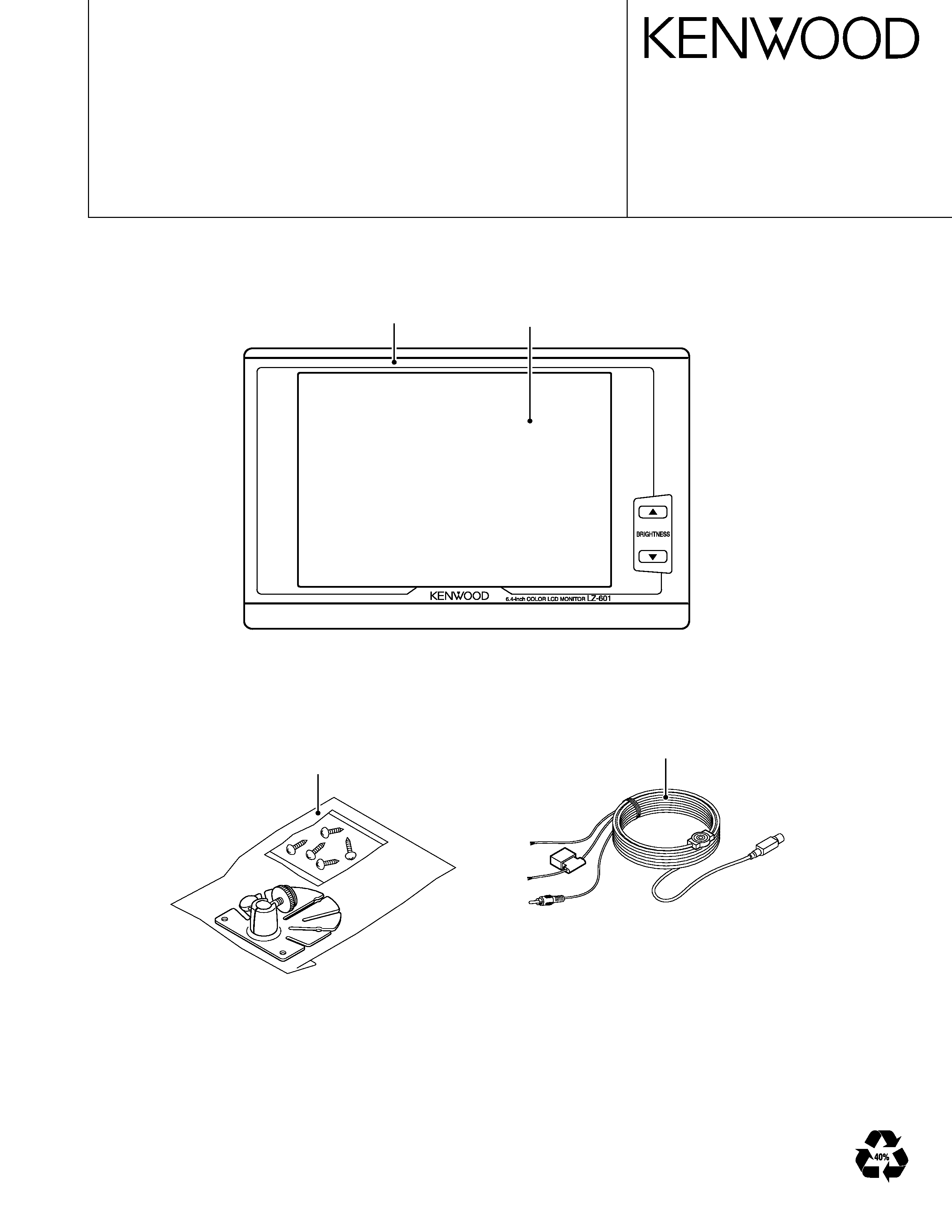
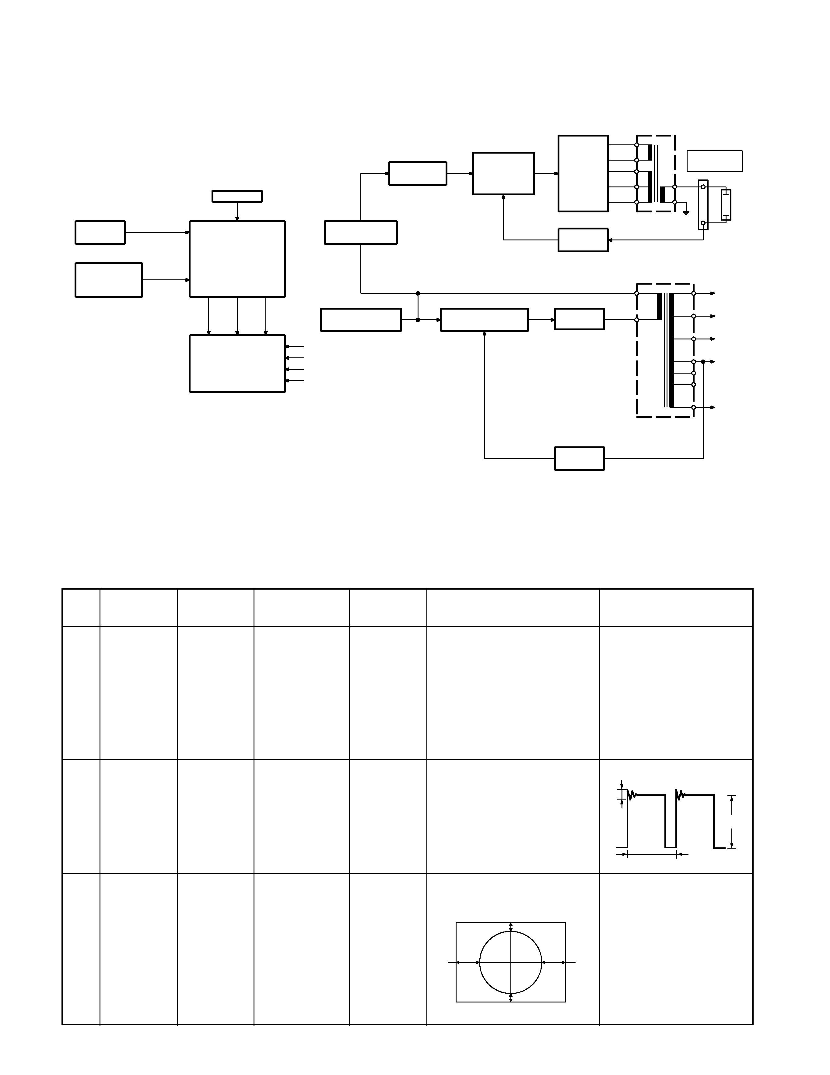
KENWOOD LZ601 Service Manual

Cover page of KENWOOD LZ601 Service Manual

Service Manual for KENWOOD LZ601, downloadable as a PDF file.

We also have owner's manual to this model.

Manual details

  • Immediate download after payment.
  • Delivered as a PDF file.
  • The manual has 12 pages
  • File size: 0.52 MB
  • Available language versions: English
  • Different language versions may vary sligthly in file size and page count.

We guarantee that...

  • our manuals are complete,
  • the manual includes circuit diagrams,
  • our manuals are checked with antivirus,
  • We'll issue refund if the manual is damaged, incomplete or unreadable (our refund policy)

Sample pages

Thumbnail of page 1Thumbnail of page 2Thumbnail of page 3Thumbnail of page 4
Thumbnail of page 5Thumbnail of page 6Thumbnail of page 7Thumbnail of page 8
Thumbnail of page 9
background image
© 2002-4 PRINTED IN JAPAN
B51-7943-00 (N) 3394
6.4 INCH ON-DASH MONITOR
LZ-601
SERVICE MANUAL
Panel
(A64-2803-08)
Liquid crystal
(B38-1102-08)
Mounting hardware
(for E type, M type)
(W01-1508-05)
DC cord
(E30-6105-05)
background image
© 2002-4 PRINTED IN JAPAN
B51-7943-00 (N) 3394
6.4 INCH ON-DASH MONITOR
LZ-601
SERVICE MANUAL
Panel
(A64-2803-08)
Liquid crystal
(B38-1102-08)
Mounting hardware
(for E type, M type)
(W01-1508-05)
DC cord
(E30-6105-05)
background image
LZ-601
2
BLOCK DIAGRAM
ADJUSTMENT
BRI
RG
B
VGH
+20V
+14V
VSH
-5V
VGL
VDD
+5V
PICTURE
CONTROL
BALANCE
WHITH
ADJUSTMENT
VIDEO PROCESS
IC201
VIDEO I/P
W201
LCD MODULE
CONTROL
HIGH VOLTAGE
IC302
POWER SOURCE
DC 12V I/P
W201
BACKLIGHT
DELAY
SWITCHING
CIRCUIT
REGULATOR
CONTROL
IC301
HIGH
VOLTAGE
OSC
VOLTAGE
CONTROL
SWITCHING PULSE
IC101
PLUSE
AMP
VOLTAGE
NFB
H.V. TRAN
T201
BACKLIGHT
LAMP
SWITCHING
TRAN
T301
+30V
+14V
+20V
+5.3V
-5V
Q101
NFB
No.
ITEM
INPUT
OUTPUT
ALIGNMENT
ALIGN FOR
STANDARD
SETTINGS
SETTINGS
POINTS
1. Adjust SVR102 so that the
output-side voltage of L102 is
L102 +5V
: 5V +0.2V, ­0V
LINE
Connect a DC
between 5.15 and 5.20V.
D101 +14V : 14V
±0.4V
1
VOLTAGE
­
voltmeter to
SVR102
2. After completing the adjust-
D102 +20V : 20V +3V, ­1V
L102 (output side)
ment of SVR102, check the
D104 +30V : 30V +3V, ­1V
voltages at D101, 102, 104
D105 ­5V : ­5V
±0.2V
and 105.
Connect a
1. Adjust SVR101 so that the
13.5
µsec±0.4µsec
OSC&
oscilloscope or
pulse duration is 13.5
µsec
2
PULSE
­
frequency
SVR101
±0.4µsec.
WIDE
counter to
Instead, it is also acceptable
CONTROL
Q101 (collector)
to adjust so that the frequency
counter reads 74kHz
±2kHz.
Adjust so that figure comes
NTSC : A : 3.0mm
±1mm
on the center position.
B : 4.0mm
±1mm
Puts a video
C : 18mm
±1mm
3
H-POS
signal for
­
H-POS
D : 19mm
±1mm
the inspection
(LCD UNIT)
PAL
: A : 4.0mm
±1mm
in VIDEO IN
B : 2.0mm
±1mm
B : 20mm
±1mm
B : 21mm
±1mm
15Vpp
13.5
µS
2Vpp
A
B
C
D
background image
LZ-601
3
No.
ITEM
INPUT
OUTPUT
ALIGNMENT
ALIGN FOR
STANDARD
SETTINGS
SETTINGS
POINTS
1. After turning the unit on, warm
it up for 15 minutes before
proceeding to the adjustment.
2. Adjust S207 so that the
voltage at IC201 pin 32 is
IC201 32pin (Bright)
2.30V
±0.1V DC.
DC : 2.30V
±0.1V
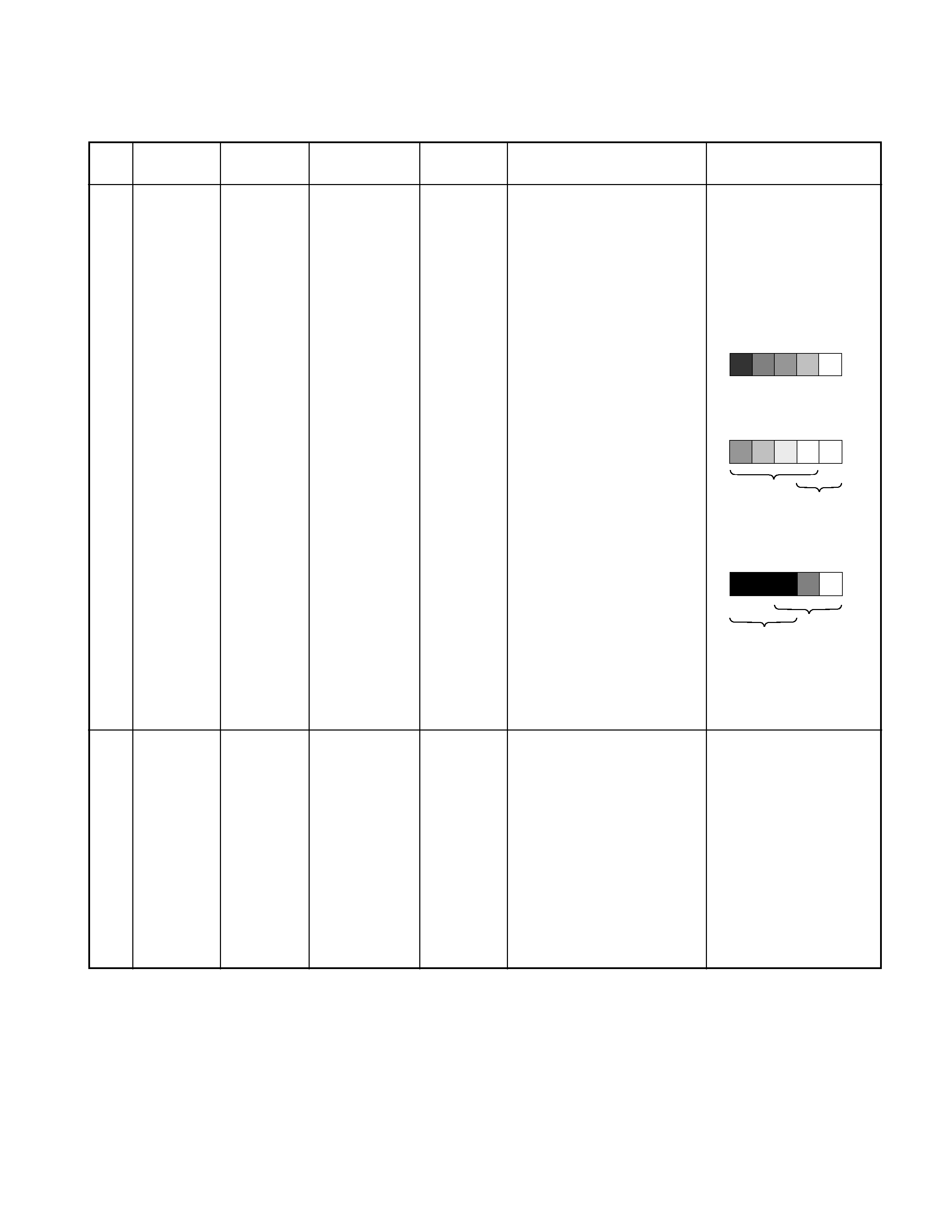
3. 1) Turn the knob (BRIGHT) to
2) BRIGHT : CENTER
the center position. (It is put
to the center position at the
moment the unit is turned
Puts a video
on.)
3) BRIGHT : MAX
signal for
Connect a DC
2) Adjust S207 so that the
4
BRIGHT
the inspection
voltmeter to
S207
second grid from the right
in VIDEO IN
IC201 (32P)
of the gray scale dims by
about 20%.
3) Turn the knob (BRIGHT) to
the MAX position and
4) BRIGHT : MIN
confirm that the three grids
from the left of the gray
scale are distinguishable.
4) Turn the knob (BRIGHT) to
the MIN position and
confirm that the three grids
on the right of the gray scale
are distinguishable.
1. After turning the unit on, warm
it up for 15 minutes before
proceeding to the adjustment.
IC201 27pin
Puts a video
2. Turn the knob (BRIGHT) to the
SVR204
WHITE
signal for
Connect a DC
S204
center position. (It is put to the
DC : 1.75V
±0.1V
5
BALANCE
the inspection
voltmeter to
S205
center position at the moment
IC201 28pin
in VIDEO IN
IC201(27P or 28P)
the unit is turned on.)
SVR205
3. R adjustment: Adjust S204 so
DC : 1.80V
±0.1V
that the background is reddish.
4. B adjustment: Adjust S205 so
that the picture is gray.
ADJUSTMENT
1
2
3
4
5
1
2
3
4
5
Distinguish
Not distinguish
1
2
3
4
5
Distinguish
Not distinguish
background image
5
A
B
C
D
E
1
2
3
4
5
6
7
PC BOARD
CONTROL UNIT
D302
D301
W801
W804
W802
W803
Z301
Q302
Q303
EB
Q305
Q
304
EB
Q306
SD
G
SD
G
Q801
Q802
Q301
IC301
IC801
C501
C304
C305
C306
C804
R810
C302
C814
C813
C811
C812
C803
R309
R303
R501
R323
R301
R302
R804
R803
R802
R801
R814
R813
R808
C801
C502
R805
R811
C303
C301
R823
R821
R822
R502
R810
C802
R805
R806
R807
R812
R308
R322
R324
F301
R315
R316
R318
R319
C309
R321
C308
R317
R320
R325
R307
R310
1
20
VIDEO
UP
DOWN
OG
V
RGB
SW802
SW801
SW302
IR501
CONTROL UNIT
D303
(COMPONENT SIDE VIEW)
(FOIL SIDE VIEW)
Refer to the schematic diagram for the values of resistors and capacitors.
CONTROL UNIT
IC
Q
Address
301
2B
801
4B
802
4B
background image
6
F
G
H
I
J
1
2
3
4
5
6
7
PC BOARD (COMPONENT SIDE VIEW)
C311
C302
C110
C103
C227
C118
C234
C122
C202
C116
C316
C313
C120
C113
C218
C101
C306
C114
R304
R305
L201
L303
L202
L203
L302
R307
C304
R303
C301
R302
R301
C117
R102
C105
C107
R106
C108
C109
R221
C111
C121
C219
C102
R247
F101
R234
R231
R230
C223
R223
R222
C210
C220
R261
R218
C217
R219
R220
R217
C216
C213
C211
C212
R246
C201
R238
C229
R239
R210
R209
C207
R240
R202
R245
R244
R206
R248
R215
C123
R248
R201
R203
C203
C204
C205
C208
R211
C206
C215
C214
R207
R208
R216
C221
C222
C224
R241
C225
C226
R233
R232
R229
R228
R227
R226
R225
R224
R214
R213
R101
R103
C112
R315
C312
RN03
RN02
C314
C315
C115
R322
R235
L301
C307
L102
L101
R320
R321
R306
R315
R314
C317
R309
R316
R310
C318
T301
C308
R311
R312
R313
C303
C305
R107
R108
R105
R104
C106
R318
C309
R317
C119
C231
C232
R26
R237
R242
R243
R204
R205
R212
C228
12
12
24
48
37
1
1
1
1
10
6
15
1
8
16
9
1
4
8
5
8
16
9
20
20
1
3
5
4
25
36
C230
C209
C267
C269
RN01
R250
X202
X201
C233
BE
EB
6
7
1
D302
W301
R308
SVR101
SVR102
S208
S209
S201
S202
S207 S206 S205 S204 S203
D102
D305
D105
W202
D205
D203
D202
D201
D104
D204
D208
D207
D206
Z301
Q301
BE
Q303
Q304
SG
D
Q307
EB
Q101
BE
Q302
B
E
Q305
B
E
Q306
EB
Q201
W201
EB
Q202
EB
Q204
EB
Q203
IC301
MAIN UNIT
IC101
IC201
IC202
IC302
T101
D304
D303
D103
D101
MAIN UNIT
IC
Q
Address
101
3G
201
6G
202
6H
301
2G
302
3H
101
4G
201
7H
202
7H
203
7F
204
7F
301
2H
302
2H
303
2H
304
2H
305
3H
306
3H
307
3H
Refer to the schematic
diagram for the values
of resistors and ca-
pacitors.

Reviews

There are no reviews of this manual yet.