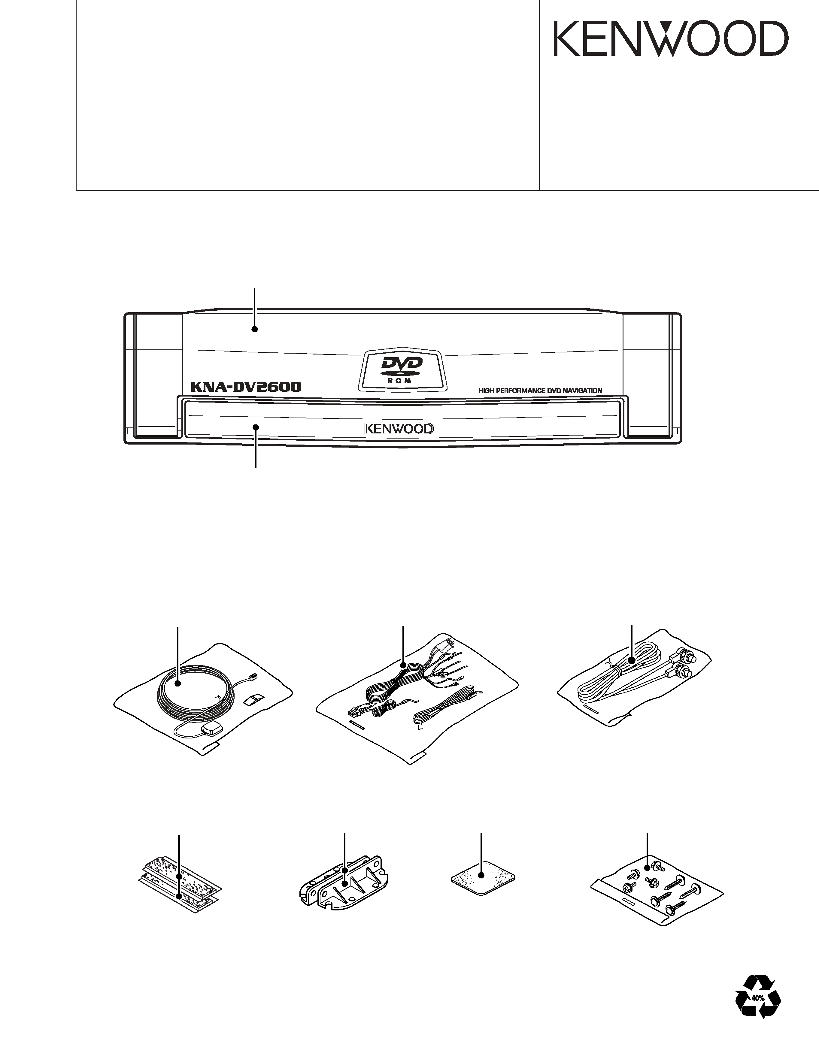
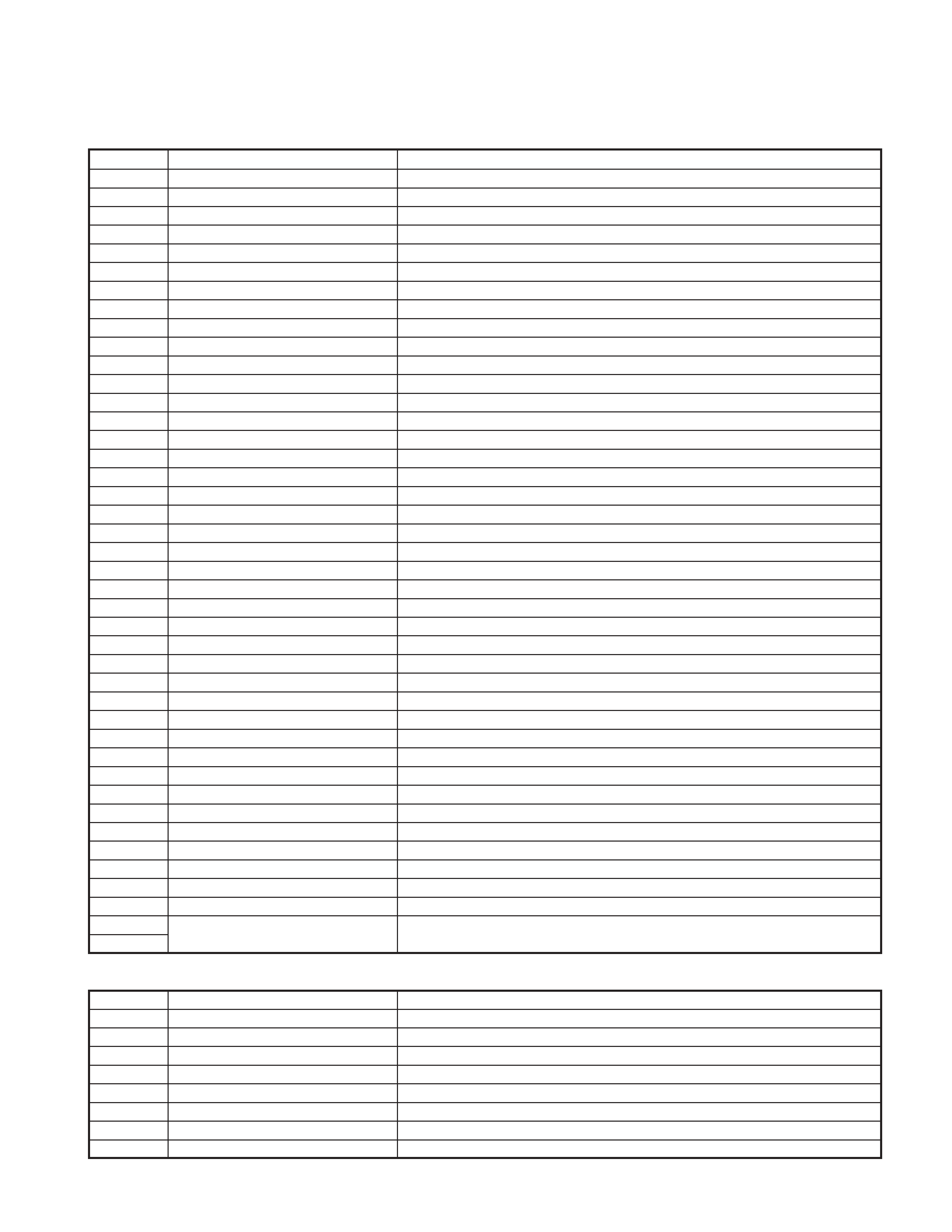
KENWOOD KNA-DV2600 Service Manual

Cover page of KENWOOD KNA-DV2600 Service Manual

Service Manual for KENWOOD KNA-DV2600, downloadable as a PDF file.

We also have owner's manual to this model.

Manual details

  • Immediate download after payment.
  • Delivered as a PDF file.
  • The manual has 32 pages
  • File size: 1.29 MB
  • Available language versions: English
  • Different language versions may vary sligthly in file size and page count.

We guarantee that...

  • our manuals are complete,
  • the manual includes circuit diagrams,
  • our manuals are checked with antivirus,
  • We'll issue refund if the manual is damaged, incomplete or unreadable (our refund policy)

Sample pages

Thumbnail of page 1Thumbnail of page 2Thumbnail of page 3Thumbnail of page 4
Thumbnail of page 5Thumbnail of page 6Thumbnail of page 7Thumbnail of page 8
Thumbnail of page 9
background image
© 2003-12 PRINTED IN JAPAN
B53-0109-00 (N) 37
DVD NAVIGATION SYSTEM
KNA-DV2600
SERVICE MANUAL
Electric circuit module
(W02-3261-05)
DC cord assy
(E30-6334-05)
Connecting cord assy
(E30-6199-05)
Screw set
(N99-1713-05)
Mounting hardware assy
(J21-9867-04)
Bracket
(J19-4596-04) x2
Magic tape
(H30-0514-05) x2
Dressing panel assy
(A21-4353-02)
Dressing panel assy
(A21-4355-03)
background image
KNA-D
V2600
2
BLOCK
DIA
GRAM
DVD
IC901,902
IC905
IC951-955,T951
IC906
MECHA.
CFC INTERFACE
POWER
SUPPLY
IC101,103,104,106,107
T101,104-111
6.7V
DVD
5V
OUTSIDE INTERFACE
3.3V
INSIDE INTERFACE
1.8V
SH4
+B
ACC
GND
SDRAM
(16MBX2)
BOOTROM
(2MB)
SRAM
(512KB)
DATA ADDRESS CONTROL SIGNAL
FMU3
IC303
IC301
T507
T502-504,506,508
IC507
IC352,353
IC451,452
GY801
DAC&
NTSC ENCODER
VOICE REFLECTION
OUTPUT INTERFACE
SIGNAL CONTROL IC
IC202
IC201
STATUS0.1
SH4
T102,103
IC110
IC105
SHCKE
RESET
WDP
B.UP
NMI
IO
-PLUS
RS422
IC402,403
IC431-433,435,437
IC802,809,810
GPS MCM
GPS ANTENNA
GYRO
VEHICLE
INTERFACE
VOICE GUIDANCE,
VOICE OUTPUT CIRCUIT
MUTE
SWITCHING
INTERFACE
NAVI VOICE/BEEP
TV VOICE
PKB
REV
ILL
SPD
DISPLAY
REFLECTION
VOICE
MONITOR
NTSC
RGB
CFC
background image
KNA-DV2600
3
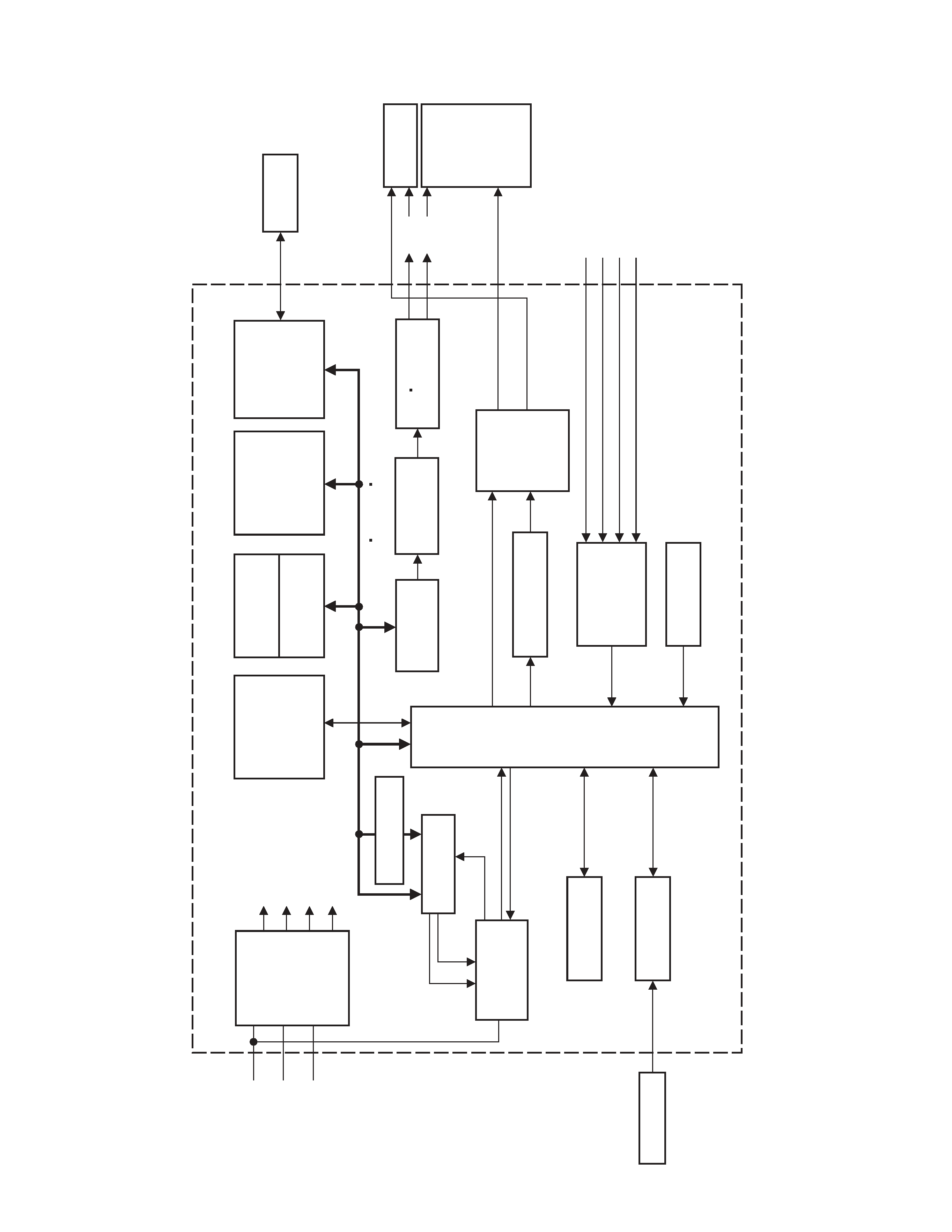
COMPONENTS DESCRIPTION
MAIN UNIT
Ref No.
Application/Function
Operation/Condition/Compatibility
IC101
Switching regulator IC
DC/DC Converter voltage controller for 6.8V and 3.3V power lines
IC103
AVR IC
3.3V output
IC104
AVR IC
5V output
IC105
Comparator
ACC & BU voltage detector
IC106
AVR IC
1.8V output
IC107
Reset IC
When momentary power down has detected, IC outputs "Lo".
IC110
Reset MI-COM
Reset controller for Main CPU and peripheral circuits
IC201
Main CPU (SH4)
IC202
Data controller
Data selector of data bus
IC301
Video DAC+NTSC encoder
IC302
NAND
Clock buffer
IC303
Graphics controller
Graphics data generator (FMU III)
IC352
Op. Amp.
Audio and beep signal adder and buffer
IC353
Analogue SW
IC357
AND
Audio mute control signal generator
IC433~437
Inverter
IC438
AVR IC
3V output
IC452
Inverter
Vehicle speed pulse waveform shaping
IC601
AVR IC
For DVD mechanism
IC606
NAND
DVD interrupt signal buffer (3V
5V level converter)
IC653
DARC decoder
FM multiple data demodulator
IC801
IO PULS
Extended IO
IC802
Inverter
IC809
Inverter
IC810
Inverter
IC901,902
SDRAM
128M
IC903
AND
SH-CKE buffer
IC904
NAND
CSRAM buffer
IC905
BOOT ROM
2M
IC906
SRAM
256K
T101
PON SW
While ACC is applied and IC110's P37 is "Hi", BU is supplied throu T101.
T102
PON SW
While ACC is applied, T102 is turned on.
T103
PON SW
When IC110's P37 becomes "Hi", T103 is turned on.
T104
Driver
T110 driver
T105,106
Driver
T111 driver
T107
BVCC3D power supply selector
T107 is turned on during BACKUP mode.
T108
BVCC3D power supply selector
T108 is turned on except BACKUP mode.
T109
Driver
T110 driver
T110
DC/DC chopper
For 6.8V AVR
T111
DC/DC chopper
For 3.3V AVR
T401
LMUTE driver
External LINE MUTE signal driver
T402
When T402's base becomes "Hi", T401 is turned on.
SUB UNIT
Ref No.
Application/Function
Operation/Condition/Compatibility
IC508
AND
TV monitor's RX/TX signal buffer
IC510
Signal selector
Remote control signal selector of TV and external remote sensor
T501
Audio mute SW
For RCA pin jack
T502
Audio signal buffer
For RCA pin jack
T505
TV audio signal mute SW
For TV monitor
T506
TV audio signal buffer
For TV monitor
T507
SYNC signal buffer
For TV monitor
T508
Mute SW driver
For audio signal muting
background image
KNA-DV2600
4
MICROCOMPUTER'S TERMINAL DESCRIPTION
IC110 : MAIN UNIT (RESET MICROPROCESSOR)
Pin No.
Pin Name
I/O
Description
Processing Operation
1P04 (TEL-CGON)
O
Power supply circuit control output
Hi : Power supply circuit ON
2
P05 (TEL-CHAG)
I
Power supply circuit ON request input
Hi : Start request
3
P06 (ACC ON)
O
ACC ON output to IO PLUS
Lo : ACC ON
4
P07 (B UP)
O
Backup condition set-up output
Lo : Backup condition
5
MODE0
-
Not used (connected to GND lines)
6
MODE1
-
Not used (connected to GND lines)
7
RST
I
RESET input (connected with RESET SW on the panel) Lo : Reset
8XOO
Resonator connection terminal
9XII
Resonator connection terminal
10
VSS
-
GND connection terminal
Connected to GND lines.
11
P37 (POWER ON)
O
P ON output
Hi : Power ON
12
P36 (WDP)
I
WDP input
Detection of pulse edge
13
P35 (ACC)
I
ACC detection input
Hi : ACC ON
14
P34 (BU)
I
Momentary power down detection
Hi : BU ON
15
P33 (CKE)
I
CKE from SH4
Lo : SDRAM self-refresh, Hi : SDRAM normal operation
16
C
-
Capacitor connection terminal
17
P32 (IOPFLWR)
O
Not used (N.C.)
18
P31 (ST1)
I
Status input 1 from SH4
19
P30 (ST0)
I
Status input 0 from SH4
20
P50 (IORES)
O
IO PLUS reset output
Lo : Reset
21
AVSS
-
GND connection terminal
Connected to GND lines.
22
P40 (VCC3ON)
O
VCC3D selection terminal (Normal)
Lo : Normal operation
23
P41 (BVC3ON)
O
VCC3D selection terminal (Backup)
Lo : Backup mode
24
P42 (RMUTE)
O
Mute output at Power ON/OFF
Lo : Mute ON
25
P43 (RES3)
O
NAVI reset output (VCC3 system reset signal)
Lo : Reset
26
P00 (SH4NMI)
O
NMI output to SH4
Hi
Lo : Back up request to SH4
27
P01 (TEL-OVER)
I
Output voltage watch of power supply circuit
Lo : Output imprudence
28
P02 (6.8VDET)
I
Output voltage watch of 6.8V power line (CDHVCC)
Hi : Output voltage OK
29
P03 (3.3VDET)
I
Output voltage watch of 3.3V power line (VCC3)
Hi : Output voltage OK
30
VCC
-
Positive power supply connection terminal
Connected to Backup power supply.
IC201 : MAIN UNIT (MAIN MICROPROCESSOR)
Pin No.
Pin Name
I/O
Description
Processing Operation
1RDY
IRDY input
2
RESET
I
Reset input
Lo : Reset
3CS0
O
Chip select 0 output
Lo : Selected (BOOT ROM)
4CS1
O
Chip select 1 output
Lo : Selected (SRAM)
5CS4
O
Chip select 4 output
Lo : Selected (IO PLUS)
6CS5
O
Chip select 5 output
Not used (N.C.)
background image
KNA-DV2600
5
Pin No.
Pin Name
I/O
Description
Processing Operation
7CS6
O
Chip select 6 output
Lo : Selected (CF Card)
8BSO
Bus start
9
VDDQ
-
Positive power supply connection terminal (+3.3V)
Connected to VCC3 lines.
10
VSSQ
-
GND connection terminal
Connected to GND lines.
11
D47
I/O
Data bus
Not used (N.C.)
12
D32
I/O
Data bus
Not used (N.C.)
13
VDD
-
Positive power supply connection terminal (+1.8V)
Connected to VCC1.8 lines.
14
VSS
-
GND connection terminal
Connected to GND lines.
15
D46
I/O
Data bus
Not used (N.C.)
16
D33
I/O
Data bus
Not used (N.C.)
17
D45
I/O
Data bus
Not used (N.C.)
18
D34
I/O
Data bus
Not used (N.C.)
19
D44
I/O
Data bus
Not used (N.C.)
20
D35
I/O
Data bus
Not used (N.C.)
21
VDDQ
-
Positive power supply connection terminal (+3.3V)
Connected to VCC3 lines.
22
VSSQ
-
GND connection terminal
Connected to GND lines.
23
D43
I/O
Data bus
Not used (N.C.)
24
D36
I/O
Data bus
Not used (N.C.)
25
D42
I/O
Data bus
Not used (N.C.)
26
D37
I/O
Data bus
Not used (N.C.)
27
D41
I/O
Data bus
Not used (N.C.)
28
D38
I/O
Data bus
Not used (N.C.)
29
D40
I/O
Data bus
Not used (N.C.)
30
D39
I/O
Data bus
Not used (N.C.)
31
VDDQ
-
Positive power supply connection terminal (+3.3V)
Connected to VCC3 lines.
32
VSSQ
-
GND connection terminal
Connected to GND lines.
33
D15
I/O
Data bus
34
D0
I/O
Data bus
35
D14
I/O
Data bus
36
D1
I/O
Data bus
37
D13
I/O
Data bus
38
D2
I/O
Data bus
39
VDD
-
Positive power supply connection terminal (+1.8V)
Connected to VCC1.8 lines.
40
VSS
-
GND connection terminal
Connected to GND lines.
41
D12
I/O
Data bus
42
D3
I/O
Data bus
43
VDDQ
-
Positive power supply connection terminal (+3.3V)
Connected to VCC3 lines.
44
VSSQ
-
GND connection terminal
Connected to GND lines.
45
D11
I/O
Data bus
46
D4
I/O
Data bus
MICROCOMPUTER'S TERMINAL DESCRIPTION

Reviews

There are no reviews of this manual yet.