3
KDV-S210P/S220P
/S230P/S240P
COMPONENTS DESCRIPTION
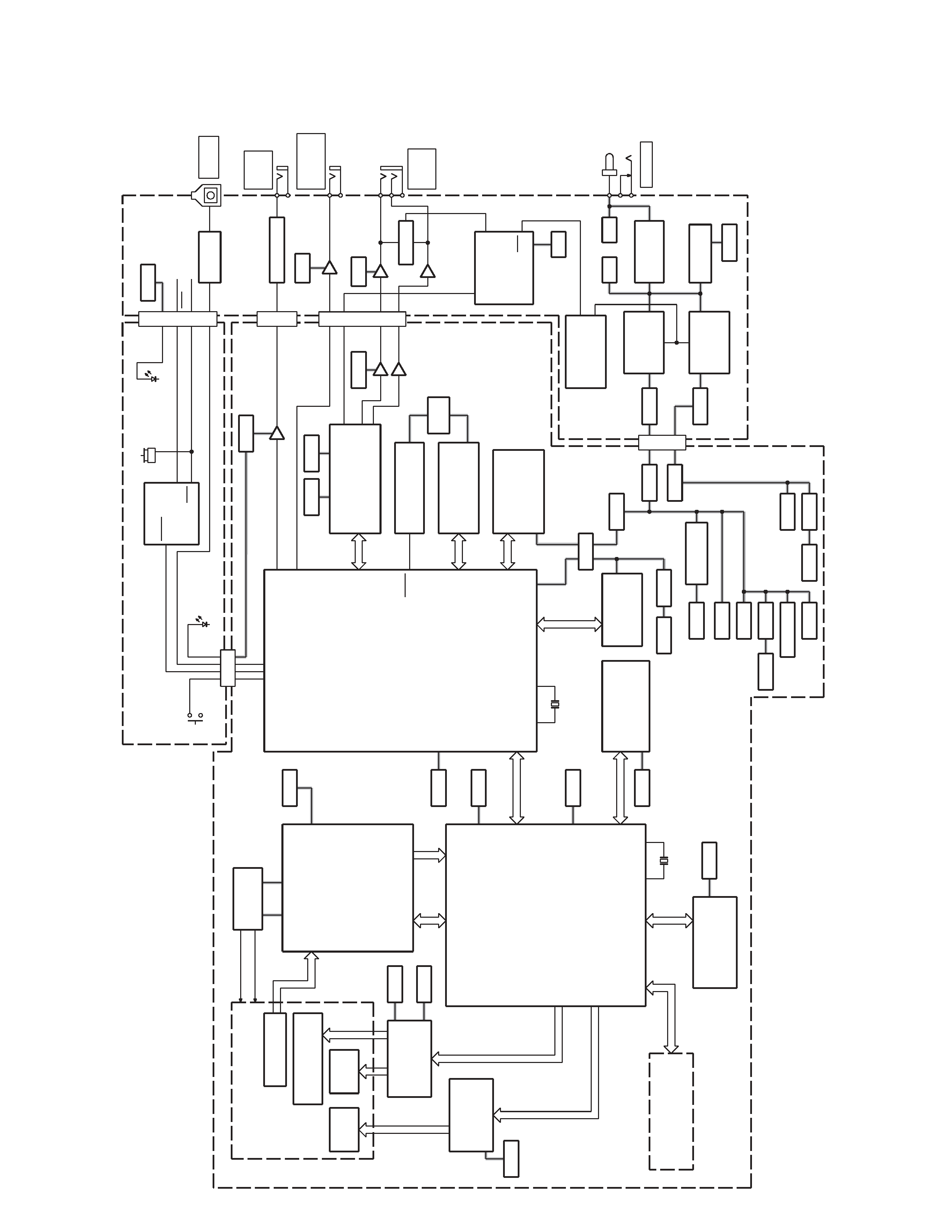
COMBO PCB
Ref. No.
Application / Function
Operation / Condition / Compatibility
MPEG decoding control
DVD MPEG images are decoded.
Dolby digital decoding control
Outputs of Dolby digital audio are decoded.
LPCM audio decoding control
LPCM audio of CD and DVD are decoded.
DVD navigation control
DVD navigation is controlled.
ATAPI communication control
ATAPI communication is control in order to control F/E.
U1
Built-in microcomputer for controlling
System as a whole and B/E are controlled. 32bit RISC microcomputer is built-in.
system and B/E system
Built-in video DAC
Video DAC is built-in to output current for composite video output from No. 106 pin.
Digital audio DAC control output
Audio signals are output from No. 32 (TWS), 33 (TSD0), 39 (MCLK), and 40 (TBCK) pins. Also,
DAC system control is conducted using No. 160 (AUX0), 161 (AUX1), and 168 (AUX6) pins.
Controls for keys and remote control
No. 162 pin is input for EJECT key. When receiving input, it is in L. No. 166 pin is for
remote control input. When receiving input, there will be pulse input.
U2
EEPROM for storing system setting
EEPROM for storing system setting information and resume information.
information and resume information
U3
Frame buffer memory
Decoding data buffer memory.
Program memory
Memory for program control.
U5
3.3V regulator
From No. 3 pin, VCC (5V) is input and from No. 2 pin, VCC33 (3.3V) is output.
U9
System reset control
Rising/Falling of VCC (5V) is detected by No. 5 pin, and L-reset output is made from No. 4 pin.
U23
For audio post LPF
CH1-side is Rch and CH2-side Lch. Constitutes a multiple feedback-type active LPF.
U27
SPDIF output, Pulse transformer driver
Inverters are connected in 3-step parallel connection for increased current capacity and
output to the pulse transformer.
U28
B/E program memory
Flash memory for storing B/E program memory.
U34
Program memory
Flash memory for storing programs.
Digital audio signal is input from No. 3 (TWS), 2 (TSD0), 16 (MCLK), and 1 (TBCK) pins.
U35
Digital audio 2ch DAC
Also, signals for DAC system control are input from No. 15 (AUX0), 14 (AUX1), and 13 (AUX6) pins.
Output for Lch analog audio is made from No. 7 pin and that for Rch is made from No. 8 pin.
DVD/CD digital servo control
Built-in DVD/CD digital servo equalizer and various timing generation circuit.
DVD/CD data decoding control
Data generation from RF of DVD/CD, error correction and control over scramble analysis
SU1
and release.
F/E section built-in system control
F/E section 8bit microcomputer for system control.
microcomputer
ATAPI communication control
ATAPI communication control with B/E.
Pickup actuator driver
Control signals for focus and tracking actuator signals of the pickup are received by No. 1 and
No. 26 pins respectively and currents are output from No. 13 and14 and No. 15 and 16 pins.
SU2
Feed motor driver
Control signals for the feed motor is received at No.6 pin and currents are output from
No. 11 and 12 pins.
Motor driver for slot loading mechanism
Control signals for slot loading mechanism motor is received at No. 23 pin and currents
are output from No. 18 and 17 pins.