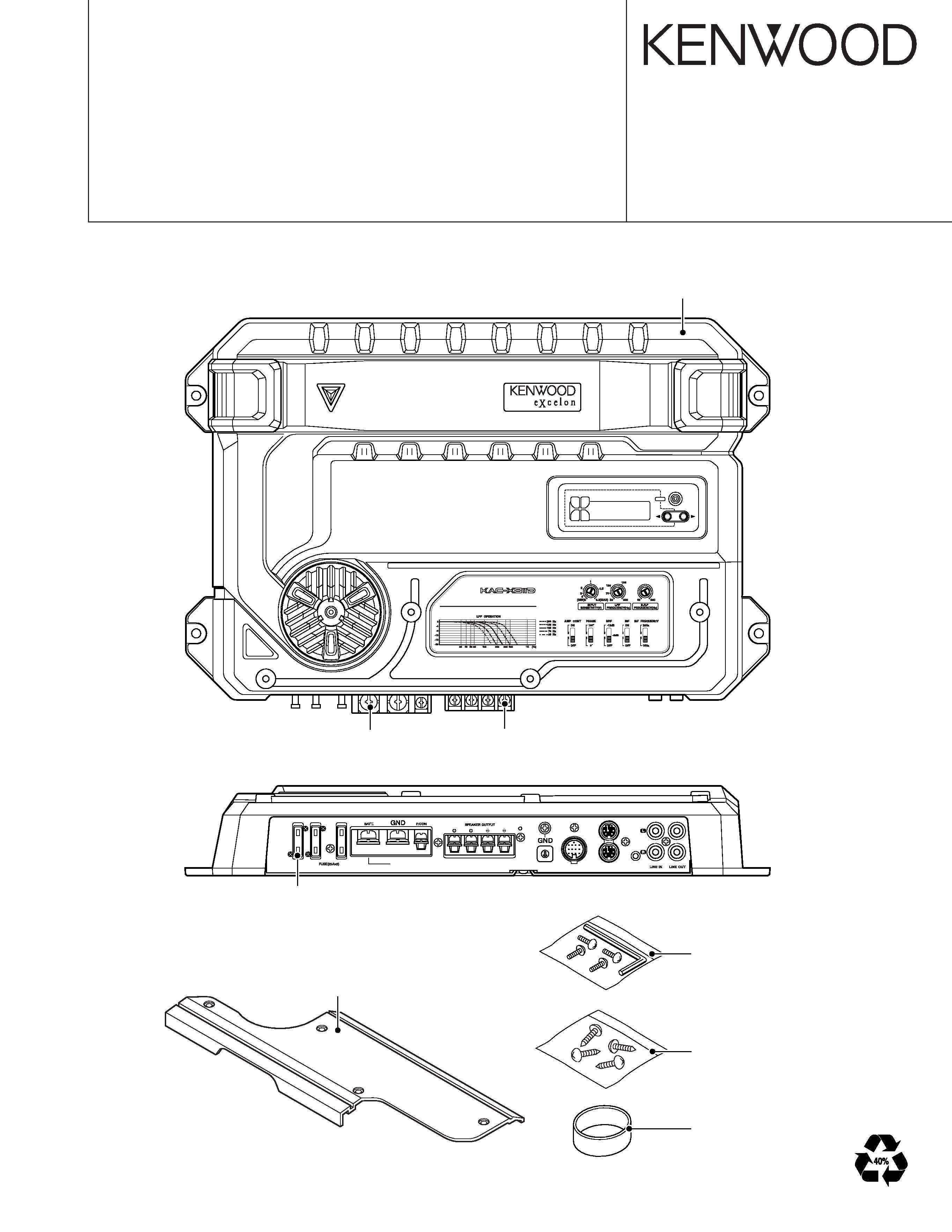
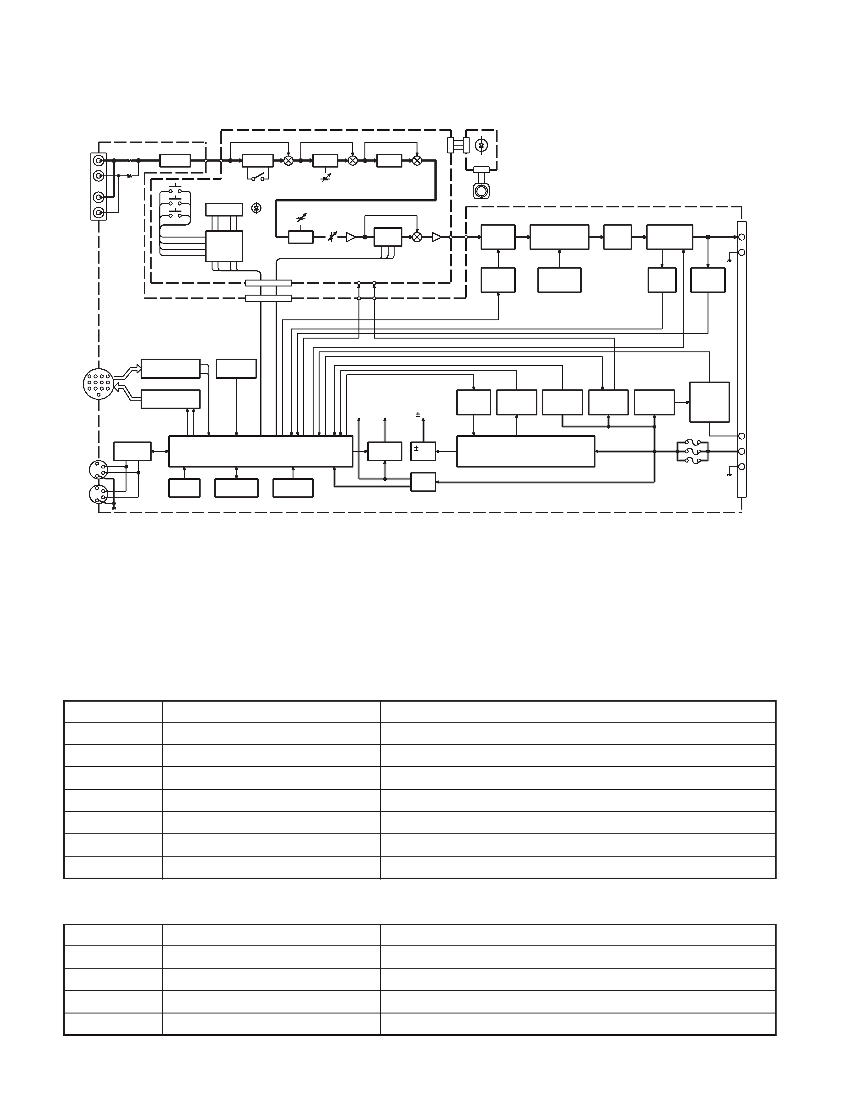
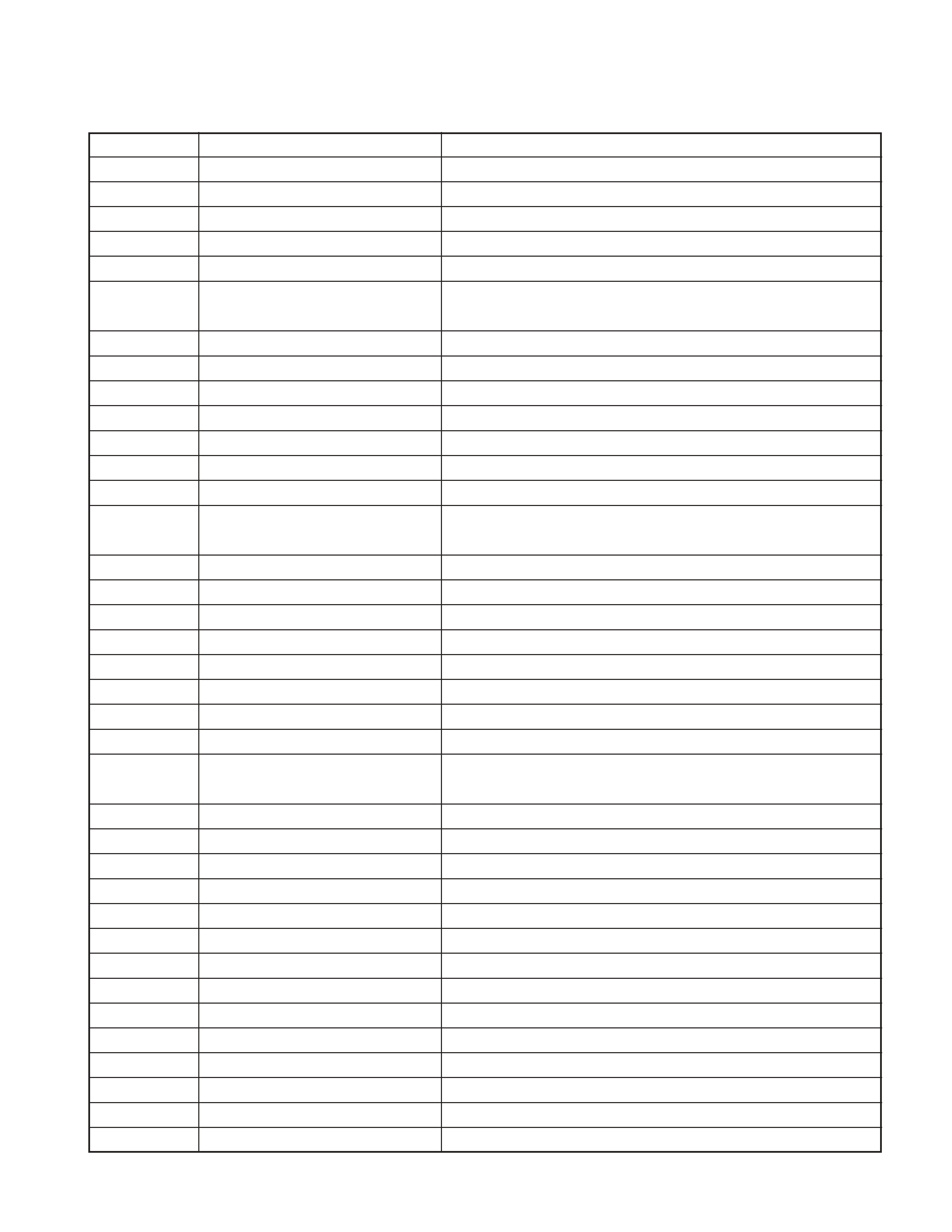
KENWOOD KACPS811D Service Manual

Cover page of KENWOOD KACPS811D Service Manual

Service Manual for KENWOOD KACPS811D, downloadable as a PDF file.

We also have owner's manual to this model.

Manual details

  • Immediate download after payment.
  • Delivered as a PDF file.
  • The manual has 24 pages
  • File size: 1.14 MB
  • Available language versions: English
  • Different language versions may vary sligthly in file size and page count.

We guarantee that...

  • our manuals are complete,
  • the manual includes circuit diagrams,
  • our manuals are checked with antivirus,
  • We'll issue refund if the manual is damaged, incomplete or unreadable (our refund policy)

Sample pages

Thumbnail of page 1Thumbnail of page 2Thumbnail of page 3Thumbnail of page 4
Thumbnail of page 5Thumbnail of page 6Thumbnail of page 7Thumbnail of page 8
Thumbnail of page 9
background image
© 2004-2 PRINTED IN JAPAN
B53-0138-00 (N) 2704
POWER AMPLIFIER
KAC-PS811D
KAC-X811D
SERVICE MANUAL
VOLT
FAN
CURR
TEMP
MENU
Subwoofer Power Amplifier
01
2
3
4 5 6 7
8
9
25
25
25
RESET
REMOTE
TO H/U
ID NUMBER
POWER IN
Screw set
(N99-1752-05)
Screw set
(N99-1577-15)
Heat sink
(F01-1751-01)
Accessory
(W01-1606-05)
Cover
(F07-1136-12): KAC-X811D
(F07-1137-12): KAC-PS811D
Screw
(N07-0003-08)
Screw
(N09-4214-08)
Fuse (25A)
(F52-0014-05)
background image
KAC-PS811D/X811D
2
BLOCK DIAGRAM
PREAMPLIFIER UNIT (X08-4170-10)
Ref. No
Application / Function
Operation / Condition / Compatibility
IC1
ISF
Cutting super-low range of audio signal
IC2 (1/4~3/4)
BRF
Cutting bandwidth of audio signal
IC2 (4/4)
INV
Phase reversal of audio signal
IC3
OP amplifier
Voltage amplification, Buffer
IC4
E-VOL
Electronic volume
IC5
LPF
Cutting high-range of audio signal
IC6
LCD driver
LCD driver
AUDIO UNIT (X09-5790-10)
Ref. No
Application / Function
Operation / Condition / Compatibility
IC1
Isolation amplifier
Prevent noise from GND potential difference
IC2 (1/2)
Triangular wave generation
Reference signal for digitizing analog signal
IC2 (2/2)
Error amplifier
Error is compensated by the feedback from output
IC3
Comparator, Triangular wave generation
Digitizing by comparison of analog signal and triangular wave
COMPONENTS DESCRIPTION
LINE
LINE IN
AMP
CONT.
DRIVER
LCD
COMPARATOR
DEAD
TIME
TRIANGLE
WAVE
LOAD
OVER
DRIVER
MUTE
DC
OFFSET
DET.
CURRENT
INPUT
VOLTAGE
CONTROL
FAN
OVER
VOLTAGE
MEASURE
DET.
SWITCH
POWER
15V
AVR
AVR
+5V
+5V
SWITCH
SWITCH
ACCRESS
ROM
CORRECT
IC
RESET
THERMAL
PROTECT
BUFFER
I2C
VOLTAGE
DET.
DOWN
P CON
DET.
AMP
MUTE
COMPARATOR
ISOLATOR
CONT
DET.
DET.
ISO
I.F.S
B.R.F
INV
L.P.F
LCD
IC4
IC3
IC3
IC5
IC2
IC2
IC1
ED1
IC6
IC1
Q10
IC2,3
IC4,5
IC2
Q9
Q52-55
78
28,37-40,42-45,48-51
Q15,18,19,21,22,27,
IC6
Q73,
IC16
Q1-4
IC15
IC11
Q20
84,110
Q106-108
IC13
Q80
IC14
Q63
Q66
Q62
D.D CON
u-COM
Q83
IC10
29,30,
Q25,26,
SP OUT
P CON
BATT
GND
OUT
to H/U
REMOTE
IND
FAN
15/25Hz
FREQ
ON/OFF
OFF/6/12
NOR/REV
ON/OFF
LEVEL
LED
FA
N
AVR 5V
SW5V
15V
FREQ
BACK
LIGHT
D
PWR
(X08-4170-10)
(X09-5790-10)
background image
KAC-PS811D/X811D
3
Ref. No
Application / Function
Operation / Condition / Compatibility
IC4,5
NAND
D class section reverse wave, deadtime, generation and rectification
IC6
Comparator
Short circuit detection of SP output
IC7
Signal amplification
For SP output short-circuit detection, send the output to comparator
IC10
Element operation control
Communication, display, protection, etc. control
IC11
Reset
Reset signal is output when voltage goes below standard voltage
IC13
DC/DC converter
Voltage on secondary side, which produces the drive signal for switching
element, will be limited to below standard voltage
IC14
Signal amplification
To have
µcom display current value, amplify potential differences of GND
IC15
Bi-directional buffer
Send/Receive data and clock between AMP
IC16
Comparator
Receive from H/U data and clock
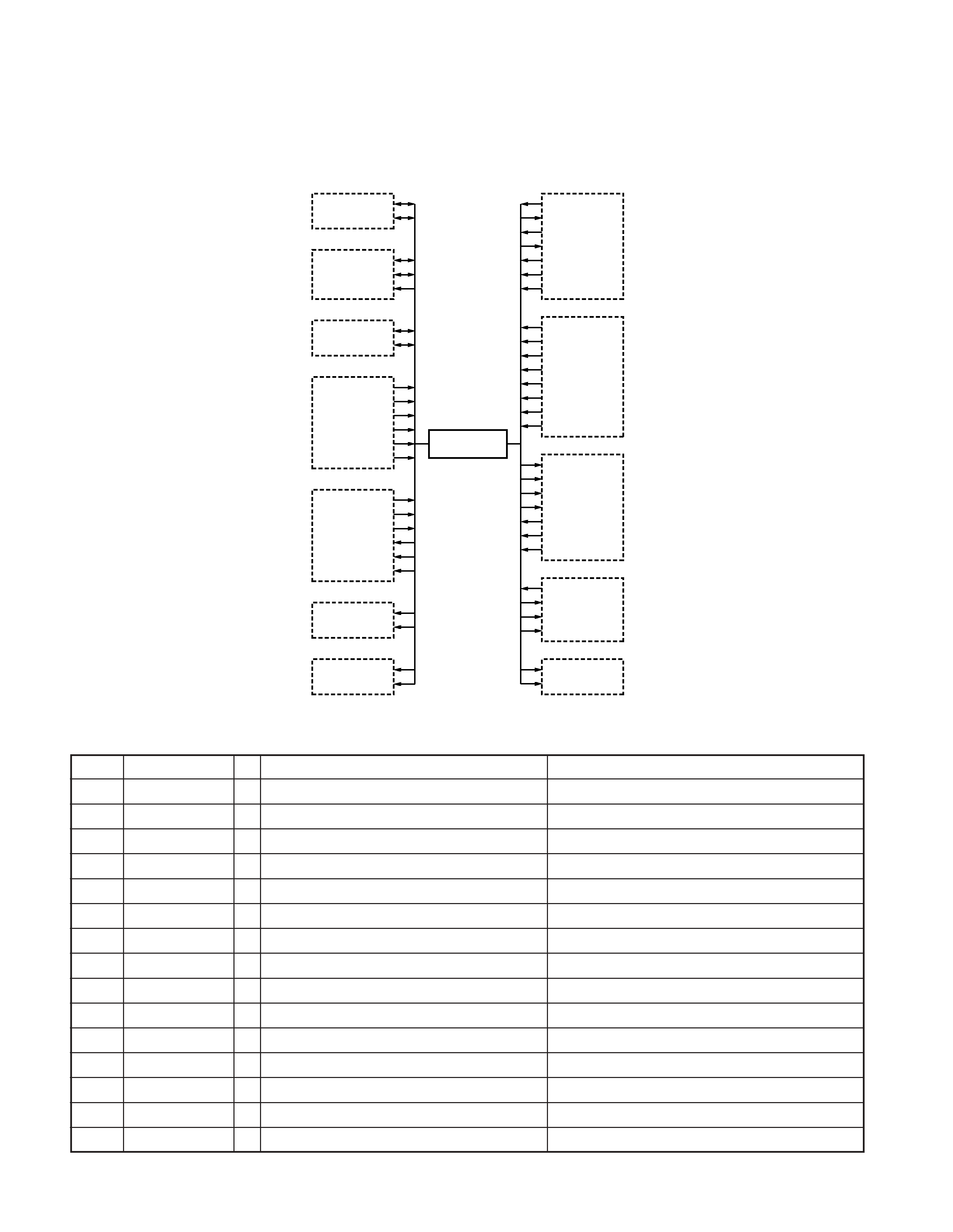
Q1,2,5,7
Digital signal transmission
Send LX-REQ-M signal to H/U
Q3,4,6,8
Digital signal transmission
Send LX-DATA-S signal to H/U
Q9
Mute
Mute drive signal generation
Q10
Mute
Turn audio signal OFF
Q15,18,19,21,22,27,
Signal amplification, switching
D class section voltage or current amplification
Q28,37~40,42~45
Q16,17
Voltage control
Match the beginning of the fall to +15V when -15V power supply is OFF
Q20
Voltage control
5V power supply ON/OFF
Q23,24,35,36,41,83
Voltage control
Fan voltage ON/OFF and limiting over voltage
Q25,29,84
AVR
+15V
Q26,30,110
AVR
-15V
Q31,33,46,109
Voltage control
D class section predrive stage power supply ON/OFF
Q47
AVR
D class section first stage supplementary power supply
Q52-55
Voltage current converter
Over current detection when SP is shorted
Q57,58,60,61,
Switching
DC/DC converter switching
Q64,65,67~70
Q59,63
Voltage control
In order to have
µcom display voltage value, send voltage to it only when 5V SW ON
Q62
Voltage detection
Pcon detection
Q66
Voltage detection
Pcon over voltage detection
Q71,72
Waveform shaping
For SP output short-circuit detection, send the output to comparator
Q73,78
Voltage detection
DC detection of output
Q74-77
Current amplification
Switching FET drive current amplification
Q79,80
Voltage control
DC/DC converter power supply ON/OFF
Q81,82
Voltage control
DC/DC converter drive waveform ON/OFF
Q88,89,98,99
Voltage control
5L digital signal reception
Q95,96
Voltage control
When Comm-SW of
µcom is ON, turn communication system power supply ON
Q97
Voltage control
Normally 15V power supply and over voltage control
Q102,111
Voltage control
When Comm-SW of
µcom is ON, turn communication system 5V power supply ON
Q103,104
Voltage control
LCD backlight and illumination LED control
Q106-108
AVR
µcom system 5V power supply.
COMPONENTS DESCRIPTION
background image
KAC-PS811D/X811D
4
AMP_SCL
LX_REQ_M
LX_REQ_S
LX_DATA_M
LX_DATA_S
LX_CLK
LX_RST
HU_BU
AD-I
AD-V
TEMP1
TEMP2
TEMP3
TEMP4
TEMP5
TEMP6
COMM-SW
D-PWER
POWER-ON
5VSW
V_DOWN
PCON
LX_CON
L_DATA_L
L_DATA_A
L_CLK
L_CE
FAN1
FAN2
AMP_SDA
AUDIO_SCL
AUDIO_SDA
AUDIO_MUTE
E2P_SCL
E2P_SDA
LCD-ILL
WHITE-LED
MUTE1
MUTE2
DIP-SW1
DIP-SW2
DIP-SW3
DIP-SW4
MODEL1
MODEL2
DC-DET
D-CUR
AB-CUR
ATT1
ATT2
ATT3
AMP
µ-com
784224YGC117
Audio control
AMP communication I/F
LX BUS I/F
Display data monitor
Power supply control
LCD driver I/F
Fan control
Destination, AMP ID
Protection control
Illumination control
Mute control
E2PROM I2C
communication
MICROPROCESSOR : 784224YGC117 (X09 : IC10)
Block Digram
Terminal Function
Pin No.
Pin Name
I/O
Function
Processing Operation Description
1~3
TEMP4~TEMP6
I
Temperature detection 4~6
4AVSS
-
GND
5
L_CE
O
CE output to LCD driver
H : LCD driver CE
6
LX_REQ_S
O
Data transmit request to H/U
H : OFF, L : ON
7AVREF1
-
DA reference voltage
8
L_DATA_L
I
Data input from LCD driver
9
L_DATA_A
O
Data output to LCD driver
10
L_CLK
O
CLK output to LCD driver
11
LX_DATA_M
I
Data input from H/U
12
LX_DATA_S
O
Data output to H/U
13
LX_CLK
I
CLK input from H/U
14
LX_BU
I
LX BUS communication, H/U connect detection
H : Not connect (Except master amplifier), L : Connect
15
NC
O
Not used
16
SDA_AMP
I/O
Data input/output AMP communication
17
NC
O
Not used
MICROCOMPUTER'S TERMINAL DESCRIPTION
background image
KAC-PS811D/X811D
5
Pin No.
Pin Name
I/O
Function
Processing Operation Description
18
SCL_AMP
I/O
CLK input/output AMP communication
19
AUDIO_SCL
I/O
CLK input/output with audio chip
20
AUDIO_SDA
I/O
Data input/output with audio chip
21
AUDIO_MUTE
O
Mute output to audio chip
H : Mute OFF, L : Mute ON
22
E2P_SCL
I/O
CLK input/output with E2PROM
23
E2P_SDA
I/O
Data input/output with E2PROM
24
NC
O
Not used
25~28
DIP-SW1~DIP-SW4
I
AMP address setting
29
MODEL1
I
Model setting 1
30
MODEL2
I
Model setting 2
31,32
NC
O
Not used
33
VSS1
-
GND
34~37
NC
O
Not used
38
LCD-ILL
O
LCD backlight switch
H : ON, L : OFF
39
WHITE-LED
O
Triangle illumination switch
H : ON, L : OFF
40
NC
O
Not used
41~43
ATT1~ATT3
O
Output attenuate due to rise in temperature 1~3
H : Attenuate, L : Not attenuate
44,45
NC
O
Not used
46
COMM-SW
O
Communication IC power switch
H : ON, L : OFF
47~50
NC
O
Not used
51
D-PWER
O
D class amplifier power supply control
H : ON, L : OFF (2ch/4ch L fixed)
52
DC-DET
I
Speaker output DC voltage detection
H : Normal, L : Abnormal
53
NC
O
Not used
54
POWER-ON
O
Amplifier power supply control
H : ON (D/AB class), L : OFF
55
5VSW
O
5VSW
H : OFF, L : ON
56
MUTE1
O
Amplifier section input stage mute control
H : OFF, L : ON
57
MUTE2
O
Driver stage pop-noise mute control
H : OFF, L : ON
58
FAN1
O
Fan rotation control
H : Operate, L : Stop
59
FAN2
O
Fan speed control
H : Low speed, L : High speed
60
RESET
-
Hard reset
H : Normal, L : Reset
61
PCON
I
Amplifier power control
H : OFF, L : ON
62
LX_CON
I
LX-BUS communication control
H : OFF, L : ON
63
LX_REQ_M
I
Data receive request from H/U
H : ON, L : OFF
64
NC
O
Not used
65
V_DOWN
I
Momentary power down detection
H : ON (Power down detection), L : OFF (L fixed)
66
NC
O
Not used
67
VSS0
-
GND
68
VD1
-
VDD
69
X2
-
Main clock input 1
70
X1
-
Main clock input 2
MICROCOMPUTER'S TERMINAL DESCRIPTION

Reviews

There are no reviews of this manual yet.