CLARION 28185 EH200 Service Manual

Cover page of CLARION 28185 EH200 Service Manual

Service Manual for CLARION 28185 EH200, downloadable as a PDF file.

Manual details

  • Immediate download after payment.
  • Delivered as a PDF file.
  • The manual has 31 pages
  • File size: 3.62 MB
  • Available language versions: English
  • Different language versions may vary sligthly in file size and page count.

We guarantee that...

  • our manuals are complete,
  • the manual includes circuit diagrams,
  • our manuals are checked with antivirus,
  • We'll issue refund if the manual is damaged, incomplete or unreadable (our refund policy)

Sample pages

Thumbnail of page 1Thumbnail of page 2Thumbnail of page 3Thumbnail of page 4
Thumbnail of page 5Thumbnail of page 6Thumbnail of page 7Thumbnail of page 8
Thumbnail of page 9
background image
PN-2701B-A
PN-2702B-A
- 1 -
Published by Service Dept.
Printed in Japan
Clarion Co., Ltd.
50 Kamitoda, Toda-shi, Saitama 335-8511 Japan
Service Dept.: 5-66 Azuma , Kitamoto-shi, Saitama 364-0007 Japan
Tel: +81-48-541-2335 / 2432 FAX: +81-48-541-2703
298-6225-00 Feb.2005
Service Manual
Model
Model
NISSAN Genuine (BOSE Type)
Cockpit Module
AM/FM Radio Stereo
6-CD Changer Deck
PN-2701B-A
(Genuine No. 28185 EH200)
(Xanavi Genuine No. CD6K-1210U)
PN-2702B-A
(Genuine No. 28185 EH500)
(Xanavi Genuine No. CD6K-1600C)
DIFFERENCE FEATURE LIST
CD section
Disc:
12cm Disc
Format:
CD-DA, MP3, WMA
MP3 Sampling rate:
MPEG1; 32kHz, 44.1kHz, 48kHz
MPEG2; 16kHz, 22.05kHz, 24kHz
MPEG3; 8kHz, 11.025kHz, 12kHz
MP3 Bit rate:
MPEG1; 48k to 320kbps/VBR
MPEG2; 24k to 160kbps/VBR
MPEG3; 24k to 160kbps/VBR
WMA Bit rate:
64k to 192kbps
Logical Format:
ISO9660 level1, 2
Romeo or Joliet
Separation:
More than 60dB(20kHz L.P.F.)
S/N ratio:
More than 80dB(20kHz, JIS-A)
Disortion:
Less tahn 0.1%(20kHz, L.P.F.)
General
Load impedance:
300 ohm / 2ch
Power output:
3.6V x 2ch
Power supply voltage: DC13.2V(10.8V to 15.6V)
Negative ground
Back-up consumption: Less than 0.3mA
Dimensions(mm):
182(W) x 100(H) x 167(D)
Weight:
Approx. 2.4kg
*
Specifications and design are subject to change without
notice for further improvement.
COMPONENTS
PN-2701B-A / PN-2702B-A
Main unit
-----------
1
PN-2701B-A
North America
PN-2702B-A
China
SPECIFICATIONS
Radio section
Tuning system:
PLL frequency synthesizer system
PN-2701B-A
AM 530kHz to 1,710kHz
FM 87.75Hz to 107.9MHz
PN-2702B-A
AM 531kHz to 1,602kHz
FM 87.5Hz to 108.0MHz
Intermediate frequency:
AM 450kHz
FM 10.7MHz
Quieting sensitivity:
AM Less than 37dBu(at 20dB S/N)
FM Less than 15dBu
(at 30dB S/N : MAIN ANT)
FM Less than 15dBu
(at 30dB S/N : SUB ANT)
Separation:
FM 22 +5/-7 dB(1kHz)
S/N ratio:
AM More than 40dB
FM More than 50dB
Model No.
Destination
background image
PN-2701B-A
PN-2702B-A
- 2 -
NOTE
*
This unit is used the special adjustment jig for measur-
ing and operation.
*
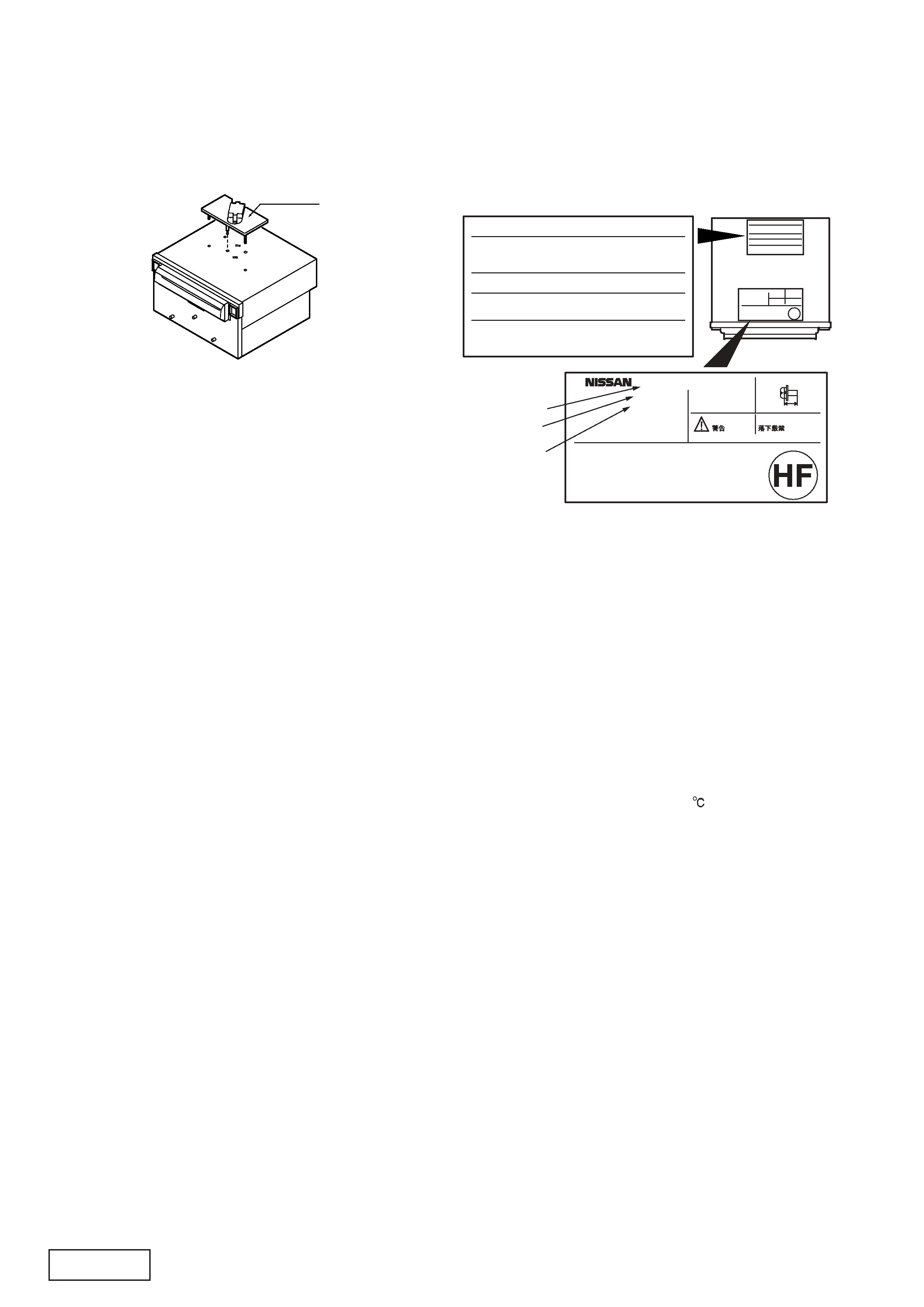
In case that the main unit or the CD changer module is
transported for repair, the lock pin(966-0653-01) must
be set to fix the mechanism assy.
CAUTIONS
Use of controls,adjustment,or performance of procedures
other than those specified herein,may result in hazardous
radiation exposure.
The compact disc player should not be adjusted or repaired
by anyone except properly qualified service personnel.
(for PN-2701B-A)
*
This product includes technology owned by Microsoft
Corporation and cannot be used or distributed without a
license from MSLGP.
*
We cannot supply PWB with component parts in prin-
ciple. When a circuit on PWB has failure, please repair
it by component parts base. Parts which are not men-
tioned in service manual are not supplied.
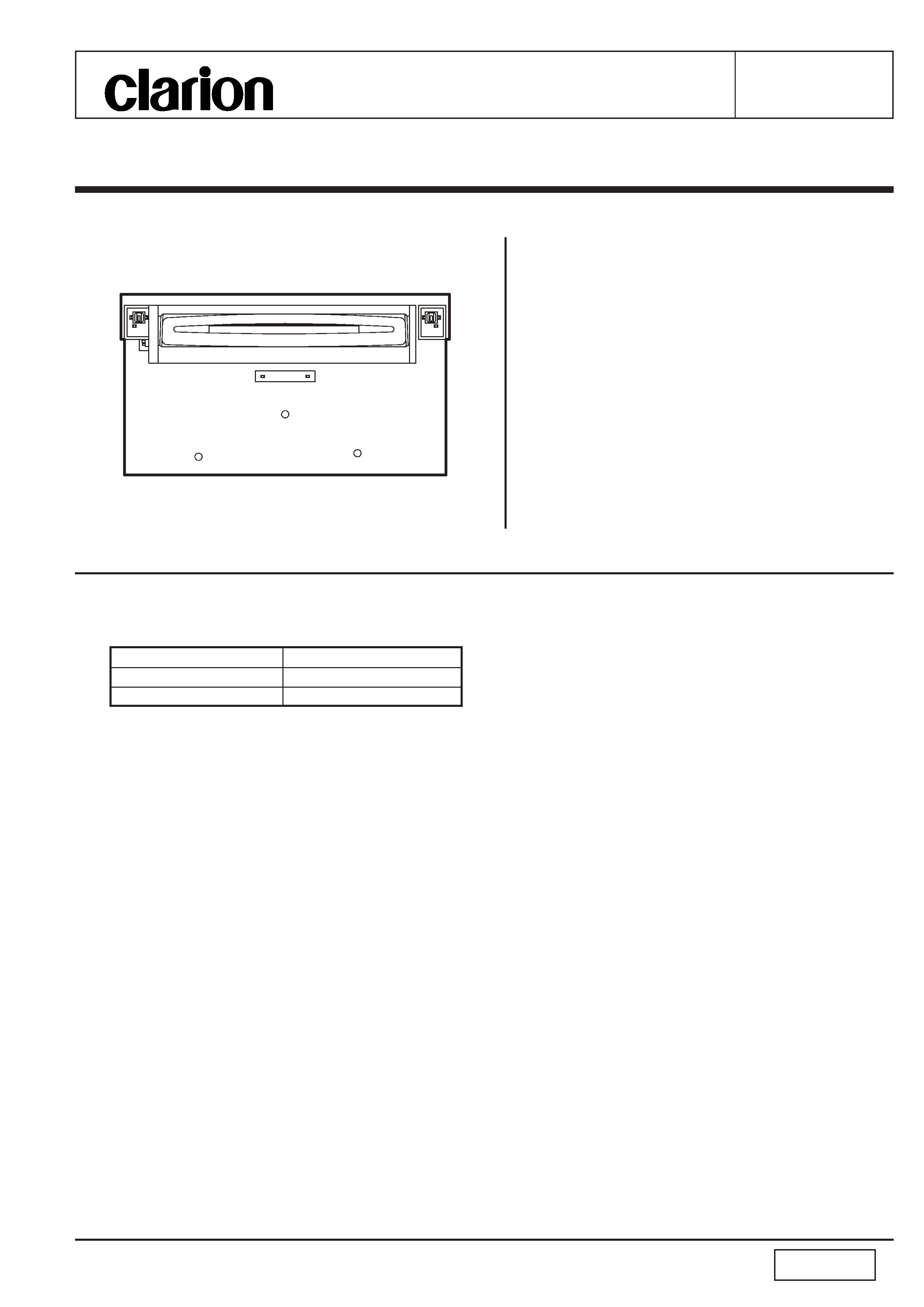
Top view
To engineers in charge of repair or
inspection of our products.
Before repair or inspection, make sure to follow the
instructions so that customers and Engineers in
charge of repair or inspection can avoid suffering
any risk or injury.
1. Use specified parts.
The system uses parts with special safety features against
fire and voltage. Use only parts with equivalent character-
istics when replacing them.
The use of unspecified parts shall be regarded as remod-
eling for which we shall not be liable. The onus of product
liability (PL) shall not be our responsibility in cases where
an accident or failure is as a result of unspecified parts
being used.
2. Place the parts and wiring back in their original positions
after replacement or re-wiring.
For proper circuit construction, use of insulation tubes,
bonding, gaps to PWB, etc, is involved. The wiring con-
nection and routing to the PWB are specially planned us-
ing clamps to keep away from heated and high voltage
parts. Ensure that they are placed back in their original
positions after repair or inspection.
If extended damage is caused due to negligence during
repair, the legal responsibility shall be with the repairing
company.
3. Check for safety after repair.
Check that the screws, parts and wires are put back se-
curely in their original position after repair. Ensure for safety
reasons there is no possibility of secondary ploblems
around the repaired spots.
If extended damage is caused due to negligence of repair,
the legal responsibility shall be with the repairing company.
4. Caution in removal and making wiring connection to the
parts for the automobile.
Disconnect the battery terminal after turning the ignition
key off. If wrong wiring connections are made with the
battery connected, a short circuit and/or fire may occur. If
extensive damage is caused due to negligence of repair,
the legal responsibility shall be with the repairing company.
5. Cautions regarding chips.
Do not reuse removed chips even when no abnormality is
observed in their appearance. Always replace them with
new ones. (The chip parts include resistors, capacitors,
diodes, transistors, etc). The negative pole of tantalum
capacitors is highly susceptible to heat, so use special care
when replacing them and check the operation afterwards.
6. Cautions in handling flexible PWB
Before working with a soldering iron, make sure that the
iron tip temperature is around 270 . Take care not to ap-
ply the iron tip repeatedly(more than three times)to the
same patterns. Also take care not to apply the tip with force.
7. Turn the unit OFF during disassembly and parts replace-
ment. Recheck all work before you apply power to the unit.
8. Cautions in checking that the optical pickup lights up.
The laser is focused on the disc reflection surface through
the lens of the optical pickup. When checking that the la-
ser optical diode lights up, keep your eyes more than 30cms
away from the lens. Prolonged viewing of the laser within
30cms may damage your eyesight.
9. Cautions in handling the optical pickup
The laser diode of the optical pickup can be damaged by
electrostatic charge caused by your clothes and body. Make
sure to avoid electrostatic charges on your clothes or body,
or discharge static electricity before handling the optical
pickup.
9-1. Laser diode
The laser diode terminals are shorted for transporta-
tion in order to prevent electrostatic damage. After
replacement, open the shorted circuit. When
removing the pickup from the mechanism, short
the terminals by soldering them to prevent this
damage.
Lock pin
966-0653-01
MANUFACTURED
.
DO NOT DROP
WARNING
MOUNT
S CRE W
M5 X 8
mm
MA X
FR E Q U E N C Y
R A N G E
A M :
530 - 1710 kHz
F M :
87.75 - 107.9 MHz
This product includes technology owned by Microsoft Corporation and
cannot be used or distributed without a license from MSLGP.
THIS PRODUCTION COMPLIES WITH DHHS RULES 21 CFR SUBCHAPTER J
APPLICABLE AT DATE OF MANUFACTURE.
THIS DEVICE COMPLIES WITH PA RT 15 OF THE FCC RULES, OPE
RATION IS SUBJECT TO THE FOLLOWING TWO CONDITIONS; (1)
THIS DEVICE MAY NOT CAUSE HARMFUL INTERFERENCE, AND (2)
THIS DEVICE MUST ACCEPT ANY INTERFERENCE RECEIVED, INCL
UDING INTERFERENCE THAT MAY CAUSE UNDESIRED OPERATION.
28185 EH200
PN-2701B
CD6K-1210U
Model No.
Xanavi No.
NISSAN No.
background image
PN-2701B-A
PN-2702B-A
- 3 -
9-2. Actuator
The actuator has a powerful magnetic circuit. If a
magnetic material is put close to it. Its character-
istics will change. Ensure that no foreign substances
enter through the ventilation slots in the cover.
SYSTEM DIAGRAM
IT-Master system (The example of PN-2701B-A.)
This audio unnit has the following connection with a navigation system and accessories.
9-3. Cleaning the lens
Dust on the optical lens affects performance. To
clean the lens, apply a small amount of isopropyl
alcohol to lens paper and wipe the lens gently.
CONNECTOR LAYOUT
J501
TH18HW-CS2
(Power/SP/STRG-Remo)
1
2
3
4
5
6
7
8
N.C.
SP FL+
SP FL-
SP RL+
SP RL-
STRG SW A
ACC
ILL CONT(*2)
9
10
11
12
13
14
15
16
ILL
N.C.
SP FR+
SP FR-
N.C.
N.C.
STRG-GND
STRG SW B
17
18
19
20
N.C.
N.C.
B/U
GND
123456789
V12
V11
V09
V08
V07
V06
V05
V03
V01
V10
V04
V02
18
17
16
15
14
13
12
11
10
19
20
J201
TH12HW (TEL)
ANT101
GT-13SHA
(ANT-IN)
J250
TH08HW
(Audio-BUS/M-CAN)
A
B
C
ANT+B
MAIN ANT
SUB ANT
h01
h02
h03
h04
h05
h06
h07
h08
Audio BUS L+
Audio BUS R+
M-CAN H
M-CAN L
Audio BUS L-
Audio BUS R-
Audio BUS GND
N.C.
h11
h12
h13
h14
h15
h16
h17
h18
N.C.
TEL VOICE+(*1)
TEL VOICE-(*1)
N.C.
N.C.
N.C.
N.C.
N.C.
h19
h20
h21
h22
TEL GND
N.C.
N.C.
N.C.
A
h01
h11 h12 h13 h14 h15 h16
h17 h18 h19 h20 h21 h22
h02 h03 h04
h05 h06 h07 h08
B
C
J820
A12MW (N-BUS)
V01
V02
V03
V04
V05
V06
N-BUS L-
N-BUS L+
N-BUS R-
N-BUS R+
N-BUS-GND
DATA-GND
V07
V08
V09
V10
V11
V12
Source-CHG
NDS-REQ1
NDS-RXD
NDS-TXD
NDS CONT
NDS-REQ2
*2 : PN-2702B-A is not connected.
*1 : PN-2702B-A is not connected.
Control unit
(DVD-NAVI)
MIC
GPS-ANT
RGB
YS,HP,VP
UART
N-BUS
AUDIO
BLUETOOTH
TWIN
N-BUS AUDIO
ANT-AMP
UART
COMPOSIT
RGB
YS,HP,VP
N-BUS
BCU
HVAC
FM-MPX
MULTIMEDIA-CAN
Audio-BUS
GSM/CDMA
COMPOSIT
GUIDE-SIG
distributor
COMPOSIT selector
RR-DISP control
OSD
TWIN BOX
VEHICLE-CAN
TEL-SIG
RSE H/P SIGNAL
Rep eat
CAMERA
CONT
Rear view
CCD
DVD-DECK
COMPOSIT
RW-RST
Rear - 8" DSIP
AUDIO
PN-2701B-A
Road map disc
Front - 8" DISP
Headphone
Remote
controller
Dolby 5.1ch
DTS Decorder
Infrared receiver
Infrared transmitter
Video distributor
for backseat
Rear entertainment
Controller
for backseat
Center
switch
Steering
remote
contorller
FR-L
FR-R
RR-L
RR-R
(CENTER)
SUB WOOFER
BOSE system
(max. 14-SP)
BOSE AMP
L/R 2ch
ANALOG 5.1ch
Satelite Radio Tuner
background image
PN-2701B-A
PN-2702B-A
- 4 -
CONNECTION OF SERVICE JIG
ADJUSTMENT
Item
Procedure
Measuring
instrument
FM noise
convergence
FM stop
sensitivity
<MAIN>
1. An antenna input is fixed to a main channel using a jig(Control panel unit).
2. Set an antenna input to main channel.
3. Input the FM 98.1/55dBu(1kHz, 22.5kHz MOD)signal. This state is standard
output(=0dB).
4. Adjust VR161 so that the output level becomes -25dB, when set the SSG output
is -20dB.
<SUB>
1. An antenna input is fixed to a sub channel using a jig(Control panel unit).
2. Set an antenna input to sub channel.
3. Input the FM 98.1/55dBu(1kHz, 22.5kHz MOD)signal. This state is standard
output(=0dB).
4. Adjust VR160 so that the output level becomes -20dB, when set the SSG output
is -20dB.
1. An antenna input is fixed to a main channel using a jig(Control panel unit).
2. Set an antenna input to main channel.
3. Input the 98.1MHz/55dBu(1kHz, 22.5kHz MOD)signal.
4. Adjust VR162 so that the input level becomes 32dB.
SSG
Digital tester
SSG
Digital tester
SUB
MAIN
ANT
M-CAN1
Molex04
SSG-1 : MAIN
PN-2701B-A / PN-2702B-A
SSG2 : SUB
ANT
M5 X 8 mm MAX
Adjustment point
VR160 (SUB)
VR161 (MAIN)
GT13
VR162
background image
PN-2701B-A
PN-2702B-A
- 5 -
EXPLANATION OF IC
052-3188-00
M30843MW-M02GP
Audio CPU
Terminal Description
pin
1: CTRST
: O : Contrast adjustment analogue output(DA).
pin
2: SPEED
: IN : Speed Pulse input.
pin
3: EEP/ST DA
:I/O: The serial data input/output for EEP and
Sub-tuner.
pin
4: EEP/ST CK
: O : The serial clock output for EEP and Sub-
tuner.
pin
5: BU DET
: IN : Backup detection signal input.
pin
6: GND
: - : Ground.
pin
7: CN VSS
: IN : Connect to VSS.
pin
8: ILL ON
: IN : Illumination ON signal input.
pin
9: SYS ON
: O : System ON signal output.
pin 10: RESET
: IN : Reset signal input.
pin 11: X out
: O : Crystal connection.
pin 12: VSS
: - : Negative voltage supply.
pin 13: X IN
: IN : Crystal connection.
pin 14: VDD
: - : Positive voltage supply.
pin 15: NMI
: IN : Connect to VDD.
pin 16: ACC IN
: IN : ACC ON flag input.
pin 17: NC
: O : Not in use.
pin 18: NC
: O : Not in use.
pin 19: TB
: IN : Time base input.
pin 20: NC
: O : Not in use.
pin 21: M CAN RX
: IN : M-CAN serial data input.
pin 22: M CAN TX
: O : M-CAN serial data output.
pin 23: Power IC Stndb : O : The standby signal output to Power IC.
pin 24: BEEP/BUZ
: O : BEEP out or the buz control.
pin 25: AMP ON
: O : AMP ON signal output.
pin 26: DIMMER
: O : PWM output.
pin 27: EEP/MT CK
: O : The clock pulse output to EEP/Main-tuner.
pin 28: EEP/MT DA
: O : The serial data output to EEP/Main-tuner.
pin 29: NDS TX
: O : The serial data output for NDS.
pin 30: NDS RX
: IN : The serial data input for NDS.
pin 31: NDS REQ 1
: IN : NDS request signal input.
pin 32: NDS CONT
: O : NDS/Automatic-changer select.
pin 33: 1&6-CD TX
: O : The serial data output for 1-CD & 6-CD-
Changer.
pin 34: 6-CD RX / CK
:I/O: The serial data input for 6-CD-Changer. Or
clock pulse output for 1-CD.
pin 35: NDS REQ 2
: IN : NDS request signal input.
pin 36: NDS S-CHG
: O : N-BUS audio signal select command out-
put.
pin 37: NC
: O : Not in use.
pin 38: NC
: O : Not in use.
pin 39: WRITE ONLY
: - : WRITE ONLY.
pin 40: NC
: O : Not in use.
pin 41: NC
: O : Not in use.
pin 42: NC
: O : Not in use.
pin 43: 1-CD RX
: IN : The serial data input from 1-CD.
pin 44: 1&6-CD REQ
: IN : The request signal input from 1-CD & 6-
CD-Changer.
pin 45: 1-CD CS
: O : The chip select signal output.
pin 46: 1-CD WUP
: O : The wakeup signal output.
pin 47: 1-CD RESET
: O : The reset signal output.
pin 48: CD ON
: O : CD ON signal output.
pin 49: Power IC Diag
: IN : Power IC Diagnosis signal input.
pin 50: LCD ON
: O : LCD ON signal output.
pin 51: KEY/LCD DO
: O : Serial data output for KEY IC or LCD IC.
pin 52: KEY/LCD CLK
: O : Clock output for KEY IC or LCD IC.
pin 53: KEY/LCD DI
: IN : Serial data input for KEY IC or LCD IC.
pin 54: KEY/LCD CE
: O : Chip Enable output for KEY IC or LCD IC.
pin 55: KEY/LCD S/R
: O : KEY IC
Standby output / LCD IC Reset
output.
pin 56: VOL-2
: IN : The volume pulse input.
pin 57: VOL-1
: IN : The volume pulse input.
pin 58: NC
: O : Not in use.
pin 59: NC
: O : Not in use.
pin 60: VDD
: - : Positive voltage supply.
pin 61: POWER-ON
: - : POWER-KEY.
pin 62: GND
: - : Ground
pin 63: RTLY-VOL2/TH : IN : Rotary volume pulse input / temperature.
pin 64: RTLY-VOL1
: IN : Rotary volume pulse input.
pin 65: MD WP
: O : MD wakeup, H = WAKE-UP, L = SLEEP.
pin 66: MD XCS
: O : MD chip select , H = CS ON.
pin 67: MD XSCK
: O : MD clock.
pin 68: CPU-MD
: O : The serial data output to MD.
pin 69: MD RESET
: O : L = RESET ON.
pin 70: MD XSRQ
: IN : MD request.
pin 71: NC
: O : Not in use.
pin 72: MD DI
: IN : The serial data input from MD.
pin 73: MD LD/RDS CK : IN : MD loading start signal input, DISC load-
ing beginning of L. And RDS clock input.
pin 74: MD ON/RDS DI : O : MD power supply control, H = Power ON.
pin 75: NC
: O : Not in use. And RDS data input.
pin 76: ST/SD/TWEET
:I/O: At AM station receiving, this port outputs
"L" by AM 900kHz receiving. At FM station
receiving, this port detects the stereo sig-
nal. And at seeking or scanning, this port
detects the SD signal.
pin 77: DSP INT
: IN : The interrupt command input from the DSP
IC.
pin 78: DSP RESET
: O : Reset signal output to the DSP IC.
pin 79: S METER
: IN : The input terminal of internal A/D convert-
er to monitor the radio field strength.
pin 80: PLL DI
: IN : Serial data input from the PLL IC.
pin 81: VFM PLL CE
: O : The chip enable signal output to the PLL
IC.
pin 82: VFM PLL DO
: O : Serial data output to the PLL IC.
pin 83: VFM PLL CK
: O : The clock pulse output to the PLL.
pin 84: VFM PLL DI
: IN : Serial data input from the PLL IC.
pin 85: VFM SD
: IN : Station detection signal input.
pin 86: VFM S METER : IN : The input terminal of internal A/D convert-
er to monitor the radio field strength.
pin 87: MD EJ/6-CD LD : IN : MD eject signal input. And 6-CD-Changer
loading start signal input.
pin 88: CD EJECT
: IN : CD eject signal input.
pin 89: PLL CK
: IN : PLL clock input.
pin 90: PLL DO
: O : Serial data output to the PLL IC.
pin 91: PLL CE
: O : The chip enable signal output to the PLL
IC.
pin 92: N REMO B
: IN : The input terminal of internal ADC for N-
remote-controller signal.
pin 93: N REMO A
: IN : The input terminal of internal ADC for N-
remote-controller signal.
pin 94: A GND
: - : Analog ground.
pin 95: NC
: O : Not in use.
pin 96: Vref
: - : Reference voltage.
pin 97: A VCC
: - : Positive voltage supply for the internal an-
alog section.
pin 98: DSP/PIC/RDS C : IN : The clock pulse input.
pin 99: DSP/PIC/RDS D : IN : The serial data input.
pin100: ANT ON
: O : Antenna ON command output.

Reviews

There are no reviews of this manual yet.