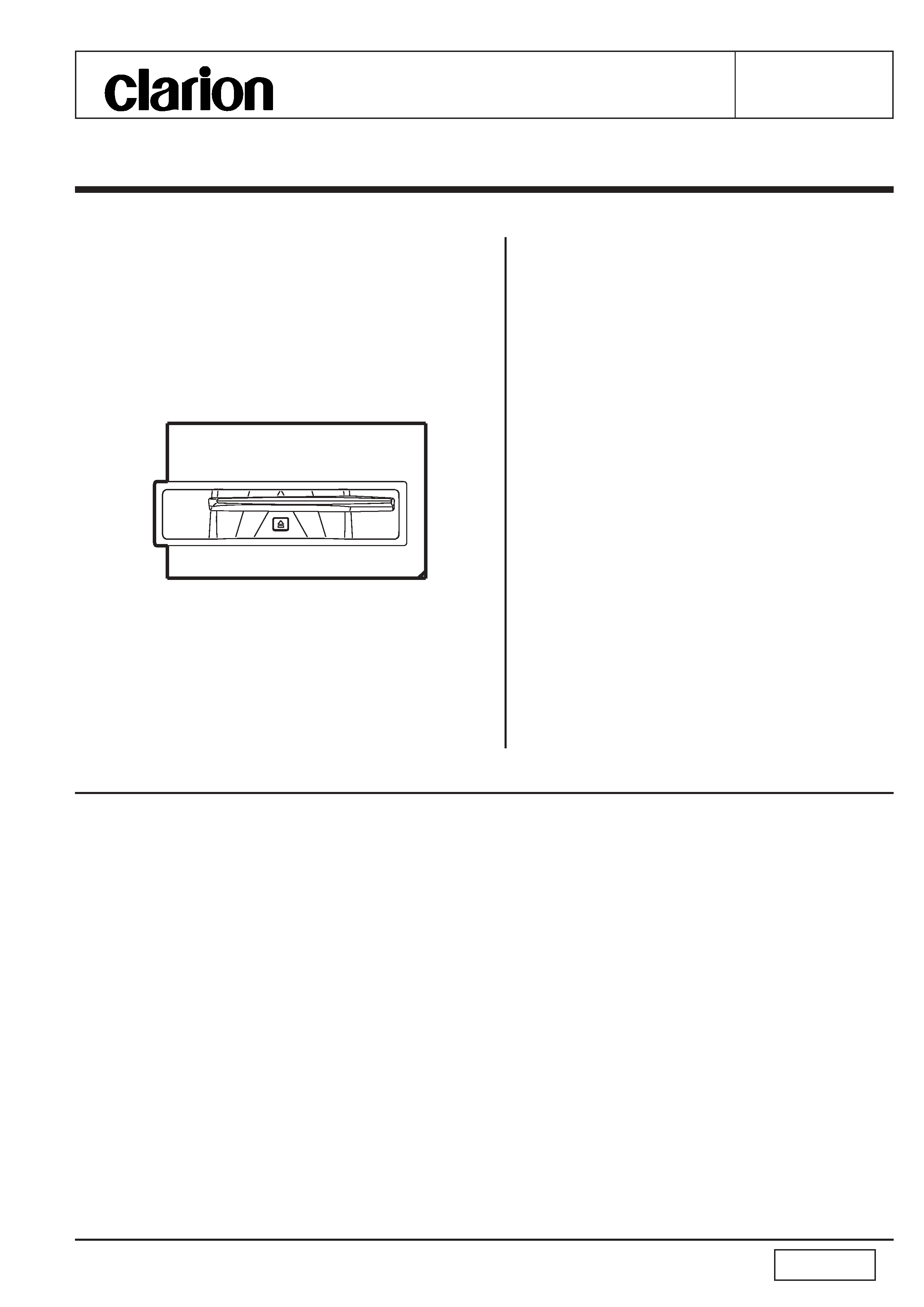
CLARION 082079 Service Manual

Cover page of CLARION 082079 Service Manual

Service Manual for CLARION 082079, downloadable as a PDF file.

Manual details

  • Immediate download after payment.
  • Delivered as a PDF file.
  • The manual has 18 pages
  • File size: 6.12 MB
  • Available language versions: English
  • Different language versions may vary sligthly in file size and page count.

We guarantee that...

  • our manuals are complete,
  • the manual includes circuit diagrams,
  • our manuals are checked with antivirus,
  • We'll issue refund if the manual is damaged, incomplete or unreadable (our refund policy)

Sample pages

Thumbnail of page 1Thumbnail of page 2Thumbnail of page 3Thumbnail of page 4
Thumbnail of page 5Thumbnail of page 6Thumbnail of page 7Thumbnail of page 8
Thumbnail of page 9
background image
PN-2540Q-C,D
PN-2540Q-E,F
- 1 -
Published by Service Dept.
Printed in Japan
Clarion Co., Ltd.
50 Kamitoda, Toda-shi, Saitama 335-8511 Japan
Service Dept.: 5-66 Azuma , Kitamoto-shi, Saitama 364-0007 Japan
Tel: +81-48-541-2335 / 2432 FAX: +81-48-541-2703
298-6218-00 Jan.2005
Service Manual
Model
Model
Model
Model
SPECIFICATIONS
Radio section
Tuning system:
PLL frequency synthesizer system
Receive range:
AM
530kHz to 1,710kHz
FM
87.9MHz to 107.9MHz
Intermediate frequency:
AM
450kHz
FM
10.7MHz
Quieting sensitivity:
AM
Less than 38dBu
FM
Less than 15dBu
Separation:
FM
22dB +5/-7dB(1kHz)
Auto tuning stop sensitivity(DX):
AM
42dBu +6/-6dBu(600kHz)
39dBu +6/-6dBu
(1000Hz,1400Hz)
FM
32dBu +6/-6dBu
NISSAN Automobile Genuine
AM/FM Radio CD Deck
PN-2540Q-C
(Genuine No. 28185 5Z005)
(VISTEON No. 18C815-ADPG05)
From Serial No.082079
PN-2540Q-D
(Genuine No. 28185 5Z006)
(VISTEON No. 18C815-ADPC62)
From Serial No.083148
PN-2540Q-E
(Genuine No. 28185 5Z010)
(VISTEON No. VP5NAX-18C815-ABPG05)
PN-2540Q-F
(Genuine No. 28185 5Z011)
(VISTEON No. VP5NAX-18C815-ABPC62)
CD section
Disc:
12cm,8cm Disc
Separation:
More than 50dB
S/N ratio:
More than 65dB
General
Load impedance:
2 ohm/4ch
Power output:
40W x 4
Power supply voltage: DC13.2V(10.8V to 15.6V)
Negative ground
Back-up consumption: Less than 0.1mA
Dimensions(mm):
180(W) x 106.4(H) x 148.4(D)
Weight:
Approx. 1.7kg
COMPONENTS
PN-2540Q-C,D,E,F
Main unit
-----------
1
background image
PN-2540Q-C,D
PN-2540Q-E,F
- 2 -
NOTE
*
We cannot supply PWB with component parts in prin-
ciple. When a circuit on PWB has failure, please repair it
by component parts base. Parts which are not mentioned
in service manual are not supplied.
*
Specifications and design are subject to change without
notice for further improvement.
CAUTIONS
Use of controls, adjustment, or performance of procedures
other than those specified herein, may result in hazardous
radiation exposure.
The compact disc player should not be adjusted or repaired
by anyone except properly qualified service personnel.
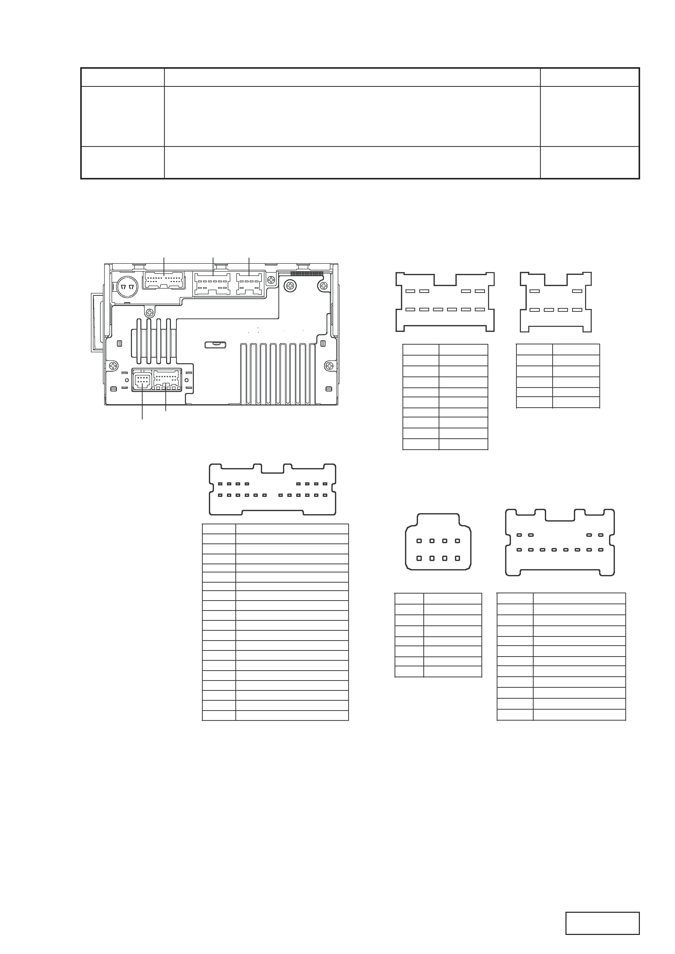
Top view of main unit
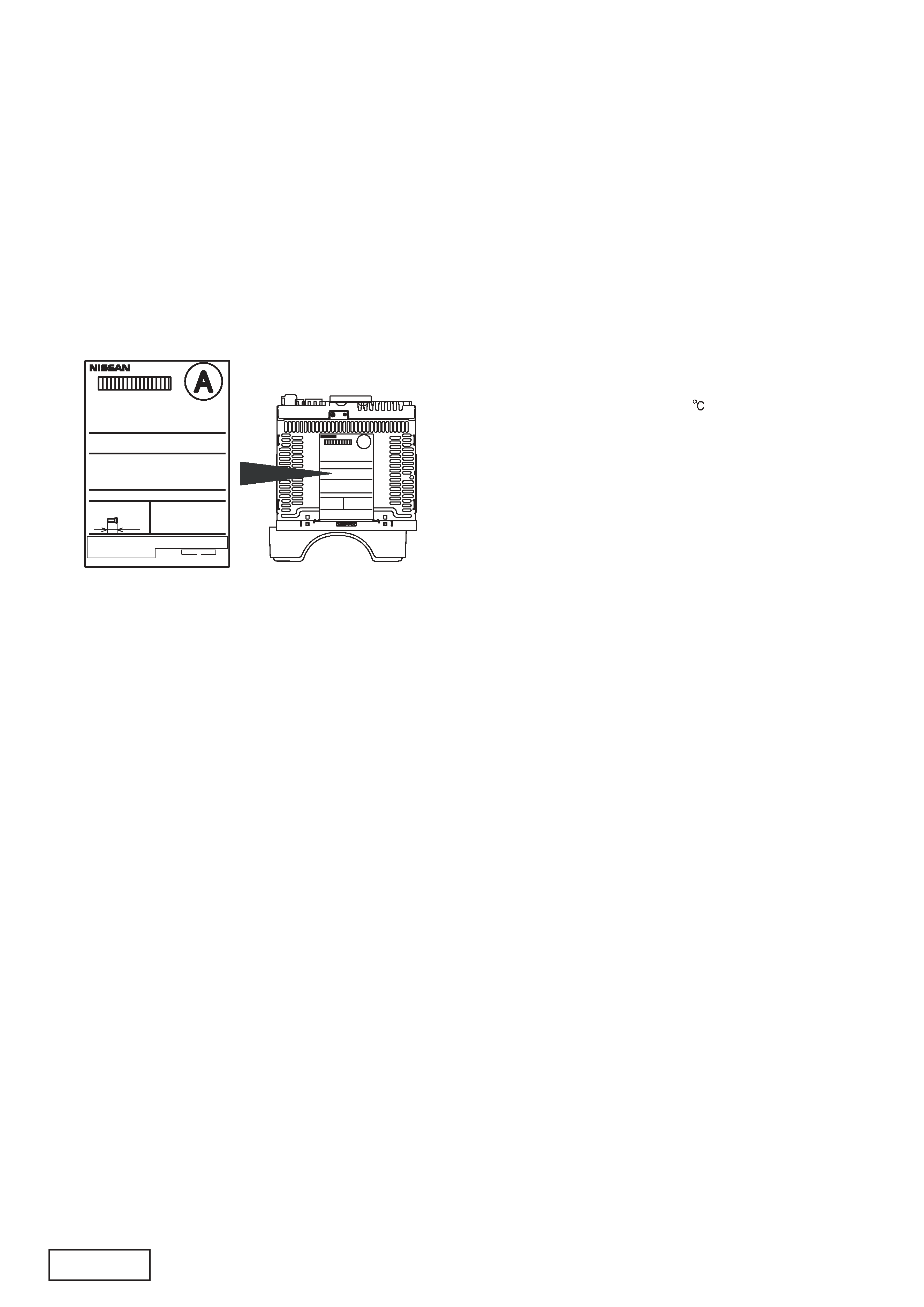
MANUFACTURED
AM: 530k Hz - 1710k Hz
ISO
(FLAT MACHINESCREW)
M5
PART No.
FM: 87. 75MHz - 107. 9MHz
FREQUENCY RANGE
THI S DEVI CE COMPLI ES WI TH PART15 OFTHE FCC
RULES. OPERATI ON I S SUBJ ECT TO THE FOLLOWING
TWO CONDI TI ONS: ( 1) THI S DEVI CE MAY NOT CAUSE
HARMFUL I NTERFERENCE. AND( 2) THI S DEVI CE MUST
ACCEPT ANY I NTERFERENCE RECEI VED, I NCLUDI NG
I NTERFERENCE THAT MAY CAUSE UNDESI RED
OPERATI ON.
THI S PRODUCTI ON COMPLI ES WI TH DHHS RULES 21 CFR
SUBCHAPTER J APPLI CABLE AT DATE OF MANUFACTURE.
MOUNT SCREW
8mm MAX
MODEL NO
P/ N
SERI AL NO.
12V( - ) GROUND
PN-2540Q
VISTEON NO.
To engineers in charge of repair or
inspection of our products.
Before repair or inspection, make sure to follow the
instructions so that customers and Engineers in
charge of repair or inspection can avoid suffering
any risk or injury.
1. Use specified parts.
The system uses parts with special safety features against
fire and voltage. Use only parts with equivalent character-
istics when replacing them.
The use of unspecified parts shall be regarded as remod-
eling for which we shall not be liable. The onus of product
liability (PL) shall not be our responsibility in cases where
an accident or failure is as a result of unspecified parts
being used.
2. Place the parts and wiring back in their original positions
after replacement or re-wiring.
For proper circuit construction, use of insulation tubes,
bonding, gaps to PWB, etc, is involved. The wiring con-
nection and routing to the PWB are specially planned us-
ing clamps to keep away from heated and high voltage
parts. Ensure that they are placed back in their original
positions after repair or inspection.
If extended damage is caused due to negligence during
repair, the legal responsibility shall be with the repairing
company.
3. Check for safety after repair.
Check that the screws, parts and wires are put back se-
curely in their original position after repair. Ensure for safety
reasons there is no possibility of secondary ploblems
around the repaired spots.
If extended damage is caused due to negligence of repair,
the legal responsibility shall be with the repairing company.
4. Caution in removal and making wiring connection to the
parts for the automobile.
Disconnect the battery terminal after turning the ignition
key off. If wrong wiring connections are made with the bat-
tery connected, a short circuit and/or fire may occur. If ex-
tensive damage is caused due to negligence of repair, the
legal responsibility shall be with the repairing company.
5. Cautions regarding chips.
Do not reuse removed chips even when no abnormality is
observed in their appearance. Always replace them with
new ones. (The chip parts include resistors, capacitors,
diodes, transistors, etc). The negative pole of tantalum
capacitors is highly susceptible to heat, so use special care
when replacing them and check the operation afterwards.
6. Cautions in handling flexible PWB
Before working with a soldering iron, make sure that the
iron tip temperature is around 270 . Take care not to ap-
ply the iron tip repeatedly(more than three times)to the
same patterns. Also take care not to apply the tip with force.
7. Turn the unit OFF during disassembly and parts replace-
ment. Recheck all work before you apply power to the unit.
8. Cautions in checking that the optical pickup lights up.
The laser is focused on the disc reflection surface through
the lens of the optical pickup. When checking that the la-
ser optical diode lights up, keep your eyes more than 30cms
away from the lens. Prolonged viewing of the laser within
30cms may damage your eyesight.
9. Cautions in handling the optical pickup
The laser diode of the optical pickup can be damaged by
electrostatic charge caused by your clothes and body. Make
sure to avoid electrostatic charges on your clothes or body,
or discharge static electricity before handling the optical
pickup.
9-1. Laser diode
The laser diode terminals are shorted for transporta-
tion in order to prevent electrostatic damage. After
replacement, open the shorted circuit. When remov-
ing the pickup from the mechanism, short the termi-
nals by soldering them to prevent this damage.
9-2. Actuator
The actuator has a powerful magnetic circuit. If a
magnetic material is put close to it. Its characteris-
tics will change. Ensure that no foreign substances
enter through the ventilation slots in the cover.
9-3. Cleaning the lens
Dust on the optical lens affects performance. To
clean the lens, apply a small amount of isopropyl
alcohol to lens paper and wipe the lens gently.
background image
PN-2540Q-C,D
PN-2540Q-E,F
- 3 -
ADJUSTMENT
Item
Procedure
Measuring
instrument
DESCRIPTION OF CONNECTORS
FM
Diversity
Noise
convergence
1. Use only Main side of the diver antenna receptacle.
2. SSG input the 98.1MHz(1kHz, 30% MOD) signal of Main side.
3. Connect a digital tester to TP101(DIV-TP).
4. Adjust VR101 so that the TP101 voltage shown 0V by input 25dBu and more than
2V by input 26dBu.
1. Input a 98.1MHz/55dB(1kHz, 30% MOD)signal. (0dB=1.4V)
2. Adjust the output to -22dB by VR104 when the SSG output is set -20dBu.
SSG
Digital tester
SSG
Milli-volt meter
30
29
27
25
23
21
22 24 26 28
31 32
38 40
36
34
33 35 37 39
J350 A20 MW
DATA EARTH
SAT-LCH (-)
42
43
44
45
46
47
48
49
50
51
52
41
SAT-LCH (+)
SAT-RCH (-)
SAT-RCH (+)
SHIELD-EARTH
NC (VPP)
SLAVE-REQ
SAT->COMB (RXD)
COMB-SAT (TXD)
NC
NC
J550 A12 MW
41 43
42 44
45 46
50 52
47 48 49 51
70 72 74 76
71 73 75 77
TEL GND
GND
71
72
73
74
75
76
77
70
NC
RX
TX
TEL ON
TEL IN (-)
TEL IN (+)
J551 A8 MW
HP OUT L-
REM-A (RSC)
22
23
24
25
26
27
28
29
30
31
32
33
34
35
36
37
38
39
40
21
REM-B (RSC)
REM-C (RSC)
REM-D (RSC)
REMOTE GROUND
HP OUT L+
HP OUT R-
HP OUT R+
SHIELD GROUND
REM ENABLE (RSC)
SWITCH +B
NC
FES LCH INPUT (-)
FES LCH INPUT (+)
FES RCH INPUT (-)
FES RCH INPUT (+)
SHIELD GROUND
DVD-ON/OFF (HU- > DVD)
AUDIO-ON(DVD-> COM)
J900 NS10 MW
ANT
GND
2
3
4
5
6
7
8
9
10
1
ACC
ILL-
ILL+
B/U
FR-
FR+
FL-
FL+
1
3
5
6
7
9
2
4
8
10
J900 NS06 MW
RR+
GND
12
13
14
15
16
11
NC
RL-
RL+
RR-
15
14
13
11
16
12
A20 MW NS10 MW NS06 MW
A8 MW
A12 MW
MAIN
SUB
ANT
background image
PN-2540Q-C,D
PN-2540Q-E,F
- 4 -
EXPLANATION OF IC
052-3179-03
uPD703033BYGC-J24-8EU
System Controller
052-3179-04
uPD703033BYGC-J46-8EU
System Controller
052-3179-04 improves performances, such as the operativity of 052-
3179-03.
Therefore, 052-3179-04 is compatible to 052-3179-03.
The main differences get with the next's.
. A default setup of SCV of 052-3179-03 is ON.
. A default setup of SCV of 052-3179-04 is OFF.
Terminal Description
pin
1: PLL DO
: O : Serial data output to the PLL IC.
pin
2: PLL CLK
: O : The clock pulse output to the PLL IC.
pin
3: DCU RX
: IN : The serial data input from DCU.
pin
4: DCU TX
: O : The serial data output to DCU.
pin
5: NU
: - : Not in use.
pin
6: E VDD
: - : Positive supply voltage.
pin
7: E VSS
: - : Ground.
pin
8: BEEP
: O : Beep out.
pin
9: NU
: - : Not in use.
pin 10: CD CONNECT
: IN : CD connection check signal input.
pin 11: BUS 0
:I/O: CD IC Data input / output.
pin 12: BUS 1
:I/O: CD IC Data input / output.
pin 13: BUS 2
:I/O: CD IC Data input / output.
pin 14: BUS 3
:I/O: CD IC Data input / output.
pin 15: BUS CLCK
: O : Clock pulse output to the CD IC.
pin 16: CCE
: O : The chip enable signal output.
pin 17: CD RESET
: O : The reset pulse output to the CD IC.
pin 18: IC VPP
: IN : For Renewal of the flash memory.
pin 19: S STOP
: IN : Inside limit signal input from the CD mech-
anism.
pin 20: CHU SW
: IN : CD disc chucking signal input.
pin 21: TR B
: IN : Photo sensor signal input from the CD
mechanism.
pin 22: TR A
: IN : Photo sensor signal input from the CD
mechanism.
pin 23: LD CONT
: IN : Loading control signal input.
pin 24: LD MUTE
: O : Muting signal output to the CD mechanism.
pin 25: GS1 TEST
: O : Test data output.
pin 26: NU
: - : Not in use.
pin 27: NU
: - : Not in use.
pin 28: NU
: - : Not in use.
pin 29: NU
: - : Not in use.
pin 30: NU
: - : Not in use.
pin 31: RESET
: IN : Reset signal input.
pin 32: NU
: - : Not in use.
pin 33: NU
: - : Not in use.
pin 34: REG C
: - : The capacitor connection.
pin 35: X 2
: - : The crystal connection.
pin 36: X 1
: - : The crystal connection.
pin 37: VSS
: - : Negative supply voltage.
pin 38: VDD
: - : Positive supply voltage.
pin 39: CLK OUT
: O : Clock pulse output.
pin 40: NU
: - : Not in use.
pin 41: NU
: - : Not in use.
pin 42: NU
: - : Not in use.
pin 43: NU
: - : Not in use.
pin 44: NU
: - : Not in use.
pin 45: NU
: - : Not in use.
pin 46: EQ SEL
: IN : Without a equalizer = "L".
pin 47: CD ON
: O : CD ON signal output.
pin 48: SYS ON
: O : System ON signal output.
pin 49: AF MUTE
: O : Audio frequency signal muting.
pin 50: AMP ON
: O : Audio power amplifier ON signal output.
pin 51: NU
: - : Not in use.
pin 52: NU
: - : Not in use.
pin 53: Audio ON
: IN : Audio ON signal input.
pin 54: DVD ENABLE
: O : DVD enable signal output.
pin 55: B VDD
: - : Positive supply voltage for the bus interface
section.
pin 56: B VSS
: - : Ground for the bus interface section.
pin 57: NU
: - : Not in use.
pin 58: REM D
: O : The remote control signal output.
pin 59: REM C
: O : The remote control signal output.
pin 60: REM B
: O : The remote control signal output.
pin 61: REM ENABLE
: O : The remote controller enable signal output.
pin 62: NU
: - : Not in use.
pin 63: NU
: - : Not in use.
pin 64: NU
: - : Not in use.
pin 65: NU
: - : Not in use.
pin 66: NU
: - : Not in use.
pin 67: NU
: - : Not in use.
pin 68: HP MUTE
: O : Head phone mute.
pin 69: NU
: - : Not in use.
pin 70: ST/TWEET
:I/O: Outputs "L" at AM 900kHz receiving. Inputs
"L" at FM stereo receiving.
pin 71: A VDD
: - : Positive supply voltage for the Analog sec-
tion.
pin 72: A VSS
: - : Analog ground.
pin 73: A Vref
: IN : Reference voltage for the internal ADC.
pin 74: REM A
: IN : The input terminal of the internal ADC for
the remote controller.
pin 75: NU
: - : Not in use.
pin 76: NU
: - : Not in use.
pin 77: TEST
: - : For the Test.
pin 78: NU
: - : Not in use.
pin 79: NU
: - : Not in use.
pin 80: NU
: - : Not in use.
pin 81: NU
: - : Not in use.
pin 82: NU
: - : Not in use.
pin 83: NU
: - : Not in use.
pin 84: NU
: - : Not in use.
pin 85: DSP DATA
: IN : DSP serial data input.
pin 86: NU
: - : Not in use.
pin 87: RDS CLK
: IN : RDS clock pulse input.
pin 88: ACC IN
: IN : ACC ON flag input.
pin 89: TEL ON
: IN : Telephone ON signal input.
pin 90: CD EJECT SW : IN : CD-Eject switch signal input.
pin 91: SBSY
: IN : Sub code block synchronous signal detec-
tion input.
pin 92: NU
: - : Not in use.
pin 93: DSP RESET
: O : Reset signal output to the DSP IC.
pin 94: DSP DATA
: O : Serial data output to the digital signal pro-
cessor.
pin 95: PLL CE
: O : The chip enable signal output to the PLL
IC.
pin 96: DSP CLK
: O : The clock pulse output to DSP.
pin 97: SAT RX
: IN : SAT serial data input.
pin 98: SAT TX
: O : SAT serial data output.
pin 99: SAT REQ
: IN : The request pulse from SAT.
pin100: PLL DI
: IN : Serial data input from the PLL IC.
background image
PN-2540Q-C,D
PN-2540Q-E,F
- 5 -
M 5
X 8
m m
M A
X
5
4
3
2
6
19
21
38
7
9
10
8
16
15
1718 13
14
12
11
20
30
40
40
16
21
29
40
41
39
40
43
27
44
22
24
23
25
26
28
31
42
34
40
33
40
32
40
35
40
37
36
1
45
21
23
074-1302-08
OUTLET SOCKET(TH08)
1
24
074-1013-00
OUTLET SOCKET(A12)
1
25
076-0313-06
PLUG(6P)
1
26
076-0313-10
PLUG(10P)
1
27
331-3529-00
OUTLET HOLDER
1
28
716-0804-01
TAP SCREW(2 X6)
2
29
313-1863-00
HEAT SINK
1
30
305-0314-00
SIDE PLATE(RH)
1
31
305-0313-00
SIDE PLATE(LH)
1
32
331-3256-00
ES PLATE
1
33
929-0220-86
CD MECHANISM
1
34
331-3254-10
MECHANISM BRKT
1
35
816-2549-02
FLAT WIRE
1
36
346-0140-00
LEATHER SHEET
1
37
335-6647-00
DISC GUIDE
1
38
311-1867-00
LOWER CASE
1
39
310-1739-10
UPPER CASE
1
40
714-2606-81
MACHINE SCREW(M2.6 x 6)
15
41
714-2612-81
MACHINE SCREW(M2.6 x 12)
2
42
714-2603-81
MACHINE SCREW(M2.6 x 3)
2
43
286-6242-11
SETPLATE(Q-C)
1
286-6242-12
SETPLATE(Q-D)
286-6242-15
SETPLATE(Q-E)
286-6242-16
SETPLATE(Q-F)
44
714-2604-81
MACHINE SCREW(M2.6 x 4)
2
45
073-0774-00
TERMINAL
1
1
940-8020-02
ES. ASSY(Q-C,Q-E)
1
(EJECT BLACK COLOR)
940-8020-12
ES. ASSY(Q-D,Q-F)
1
(EJECT BEIGE COLOR)
2
-----------
SWITCH PWB
1
3
340-4401-00
LED HOLDER
1
4
001-0569-06
LED DIODE
1
5
013-3934-02
SWITCH
1
6
074-1151-06
OUTLET SOCKET(6P)
1
7
716-0778-00
WAVE SCREW(2 x 6)
3
8
-----------
MAIN PWB
1
9
076-0540-06
PLUG(6P)
1
10
074-1191-26
OUTLET SOCKET(26P)
1
11
103-2012-00
TRANSISTOR(2SD2012)
1
12
051-2037-00
POWER IC
1
13
074-1319-20
OUTLET SOCKET(A20)
1
14
074-1068-11
OUTLET SOCKET(NS10P+6P)
1
15
880-1921U
AM/FM TUNER
1
16
073-0762-90
TERMINAL
2
17
854-4561-50
EXTENSION LEAD
1
18
854-4560-50
EXTENSION LEAD
1
19
345-5336-00
CUSHION RUBBER
1
20
307-0683-15
REAR PLATE
1
WITH ANT-RECEPTACLE
21
716-0878-00
IT SCREW(M2.6 x 5)
3
22
-----------
SUB PWB
1
NO.
PART NO.
DESCRIPTION
Q'TY
NO.
PART NO.
DESCRIPTION
Q'TY
EXPLODED VIEW/PARTS LIST
Main section
Note) Some parts depend on each model.
The model name is specified in the description.
Q-C:PN2540Q-C,Q-D:PN2540Q-D,Q-E:PN2540Q-E,Q-F:PN2540Q-F,

Reviews

There are no reviews of this manual yet.